Difference between revisions of "DNA Melting Part 2: Lock-in Amplifier and Temperature Control"
Steven Nagle (Talk | contribs) (→Operational Amplifiers) |
Eliot Frank (Talk | contribs) |
||
| Line 12: | Line 12: | ||
* Adding a heating/cooling controller to your system. | * Adding a heating/cooling controller to your system. | ||
* Revising your LED driver and photodiode amplifier circuits to support lock-in signal detection. | * Revising your LED driver and photodiode amplifier circuits to support lock-in signal detection. | ||
| − | * Downloading and using a | + | * Downloading and using a Matlab GUI that implements the software portions of temperature control and lock-in detection. |
* Refining data analysis by modeling important system behaviors such as photobleaching and temperature lag. | * Refining data analysis by modeling important system behaviors such as photobleaching and temperature lag. | ||
| Line 24: | Line 24: | ||
| | | | ||
|- | |- | ||
| − | | [[Image:Electrical_Background.jpg|225 px|thumb|center| | + | | [[Image:Electrical_Background.jpg|225 px|thumb|center|GUI Raw Signals]] |
| − | | [[Image:Light_Electrical_Combined_Background.jpg|225 px|thumb|center| | + | | [[Image:Light_Electrical_Combined_Background.jpg|225 px|thumb|center|GUI Lock-in]] |
| − | | [[Image:Instrument_Light_Electrical_Combined_Background.jpg|225 px|thumb|center| | + | | [[Image:Instrument_Light_Electrical_Combined_Background.jpg|225 px|thumb|center|GUI Control Panel]] |
|- | |- | ||
|| | || | ||
| Line 37: | Line 37: | ||
|} | |} | ||
| − | A block diagram of the lock-in scheme is shown below. Implementing lock-in detection requires the ability to modulate the LED output with a carrier frequency and signal processing (in software) to recover the baseband signal. To support these functions, the LED circuit must be modified to include a feedback brightness controller. In addition, the photodiode amplifier must be modified to accommodate the change in signal frequency range. In the | + | A block diagram of the lock-in scheme is shown below. Implementing lock-in detection requires the ability to modulate the LED output with a carrier frequency and signal processing (in software) to recover the baseband signal. To support these functions, the LED circuit must be modified to include a feedback brightness controller. In addition, the photodiode amplifier must be modified to accommodate the change in signal frequency range. In the GUI, you will need to choose the LED drive and frequency parameters to support your design. |
[[Image:DNA_Lock-in_Block_Diagram_20130725.png|500 px|center|Block diagram of lock-in amplifier for DNA melting]] | [[Image:DNA_Lock-in_Block_Diagram_20130725.png|500 px|center|Block diagram of lock-in amplifier for DNA melting]] | ||
| Line 43: | Line 43: | ||
==LED modulation== | ==LED modulation== | ||
| − | The LED used in this lab can | + | [[Image:LED_Op-amp_Drive_Schematic.png|250 px|thumb|right|LED driver circuit]] |
| + | The LED used in this lab can operate up to 30mA of current when driven to its full range. In Part 1 of the lab you had used roughly the full 30 mA. For Part 2 you will drive the LED with an op-amp which will limit the current to about 10 mA. LED radiant flux — your excitation light — is proportional to current, so we will implement a controlled current source and direct it through the LED to provide a stable sample excitation. | ||
| − | To implement the current source to drive your LED, you will use | + | To implement the current source to drive your LED, you will use an LM741 op-amp<ref>[http://www.national.com/ds/LM/LM741.pdf LM741 Op-amp datasheet]</ref>, with the output connected to the LED and a current sensing feedback resistor. Out feedback setup means we are controlling the total current through the LED. The feedback voltage is directly proportional to the resistor current and because of our choice of resistor value, the current through the LED is proportional to the voltage applied to the op-amp positive input by the DAQ. (Remember the golden rules.) So we are easily able to control the current through the LED, and likewise able to control the excitation light delivered to our dsDNA specimen. |
| − | + | ||
| − | + | ||
| − | + | ||
| − | + | ||
| − | + | ||
| − | + | ||
{{Template:Safety Warning|message=As before, double check your wiring before powering the LED. The LED can be damaged by excessive current. Reduce the offset and amplitude of your driving current to protect the LED as well as to minimize photobleaching.}} | {{Template:Safety Warning|message=As before, double check your wiring before powering the LED. The LED can be damaged by excessive current. Reduce the offset and amplitude of your driving current to protect the LED as well as to minimize photobleaching.}} | ||
| − | |||
==Adjust photodiode amplifier gain and add high-pass filter== | ==Adjust photodiode amplifier gain and add high-pass filter== | ||
| Line 69: | Line 63: | ||
==Add heater controller board== | ==Add heater controller board== | ||
| − | In order to control a slow ramp up and ramp down in block and sample temperature, the pulse width modulator (PWM) technique has been implemented on the heater/cooler printed circuit board (PCB) that is provided for you. Once the correct connections have been made, you will be able to control your block temperature using the | + | In order to control a slow ramp up and ramp down in block and sample temperature, the pulse width modulator (PWM) technique has been implemented on the heater/cooler printed circuit board (PCB) that is provided for you. Once the correct connections have been made, you will be able to control your block temperature using the Matlab GUI with minimal input on your part. It is not required that you learn the details of the heater/cooler controller design and operation, but if you want to know more, please talk to an Instructor or TA. |
[[Image:HeaterCoooler_PCB_Top.JPG|400 px|thumb|center|DNA Melting Heater Controller Board]] | [[Image:HeaterCoooler_PCB_Top.JPG|400 px|thumb|center|DNA Melting Heater Controller Board]] | ||
| Line 80: | Line 74: | ||
|} | |} | ||
| − | All points of connection are labeled on the PCB. Using the reference images above, make connections between your PCB and your DAQ cable (as described in the next section) | + | All points of connection are labeled on the PCB. Using the reference images above, make connections between your PCB and your DAQ cable (as described in the next section), and also your fan. The connection to the fan itself is self-explanatory, and is labeled as "Fan+" for the red wire and "Fan-" for the black wire. |
Next, connect your TEC and the computer power supply for the TEC and fan. Do not yet switch on the Diablotek computer power supply. Connect your TEC to the 2-pin Molex male connector on the left of the board using a Part 2 (red/black wires) female connector provided on the counter in the same box as the Part 1 connector (Black/White wires). Connect the free end of the new TEC wires to your TEC stack using wire nuts as before. If your TEC is installed correctly, connect red-to-red and black-to-black. If it is upside down, reverse the connections. Now verify that the Diablotek computer power supply is not switched on. Then connect the the 4-pin connector from the Diablotek that IS NOT labeled for Part 1 to the "Diablotek" 4-pin connector labeled on the PCB. These 2-pin and 4-pin connectors are all white, in contrast to the one black connector that you used for Part 1. | Next, connect your TEC and the computer power supply for the TEC and fan. Do not yet switch on the Diablotek computer power supply. Connect your TEC to the 2-pin Molex male connector on the left of the board using a Part 2 (red/black wires) female connector provided on the counter in the same box as the Part 1 connector (Black/White wires). Connect the free end of the new TEC wires to your TEC stack using wire nuts as before. If your TEC is installed correctly, connect red-to-red and black-to-black. If it is upside down, reverse the connections. Now verify that the Diablotek computer power supply is not switched on. Then connect the the 4-pin connector from the Diablotek that IS NOT labeled for Part 1 to the "Diablotek" 4-pin connector labeled on the PCB. These 2-pin and 4-pin connectors are all white, in contrast to the one black connector that you used for Part 1. | ||
| Line 94: | Line 88: | ||
===Update the DAQ connections=== | ===Update the DAQ connections=== | ||
| − | In the DAQ connections inset above, the "Fan" connection is a 0 or 5 V signal from the DAQ, controlled by the | + | In the DAQ connections inset above, the "Fan" connection is a 0 or 5 V signal from the DAQ, controlled by the Lock-In GUI. The "Heat/Cool" connection is a 0 or 5 V signal, also sent by the DAQ and controlled by the GUI, that tells the heater/cooler logic circuits to either heat (high, 5 V) or cool (low, 0 V). The DGND slot next to both the Fan and Heat/Cool connections should be connected to the digital ground of the DAQ, which is provide using the bare wire from your DAQ connector, as described in the handout. |
| − | Next, the "On/Off" connection also accepts a 0 or 5 V signal from the DAQ. However this signal is provided a square wave of varying duty cycle. This approach forms the heart of PWM power control. When the signal is high, the power switches in the large BTN7930 half-bridge chips are configured to allow current to flow through the TEC. The Heat/Cool signal controls the direction of power flow as noted above. When the On/Off signal is low, no power flows through the switches in either direction, when it is high, power will flow. A control loop inside the | + | Next, the "On/Off" connection also accepts a 0 or 5 V signal from the DAQ. However this signal is provided a square wave of varying duty cycle. This approach forms the heart of PWM power control. When the signal is high, the power switches in the large BTN7930 half-bridge chips are configured to allow current to flow through the TEC. The Heat/Cool signal controls the direction of power flow as noted above. When the On/Off signal is low, no power flows through the switches in either direction, when it is high, power will flow. A control loop inside the Lock-In GUI implements a Proportional-Integral-Derivative (PID) controller to set both the On/Off pulse widths and the Heat/Cool signal level in such a way as to maintain a desired temperature, or follow a desired temperature profile in time. The frequency of this duty cycle is pre-set at 10 Hz so that it's overtones do not interfere with the typical 10 kHz LED modulation frequency of your lock-in amplifier. If you choose a different LED modulation frequency, you may want to adjust the PWM frequency as well. The two half-bridge chips, connected and controlled as they are here, form what is called an H-bridge. If you want to know more, please ask an Instructor or TA. |
{| class="wikitable" | {| class="wikitable" | ||
| Line 149: | Line 143: | ||
<center>[[Image:DAQ_Wire_Colors.png|450 px|thumb|center|DAQ Connection Cable]]</center> | <center>[[Image:DAQ_Wire_Colors.png|450 px|thumb|center|DAQ Connection Cable]]</center> | ||
| − | ===Update and test the | + | ===Update and test the Matlab GUI=== |
| − | + | The lock-in GUI is <code>DNALockIn.m</code>, provided for you on the course share in the <code>CourseMaterials/Labs/DNAMelting</code> folder. Be sure to make your own copy and adjust the parameters of the RTD temperature calculations as necessary. Follow the instructions in the GUI to run an experiment. | |
| − | However, before you run any experiments, verify that you have connected the PCB board to the DAQ and TEC power supply appropriately. First open the | + | However, before you run any experiments, verify that you have connected the PCB board to the DAQ and TEC power supply appropriately. First open the GUI in Matlab and start it by clicking the green "Run" arrow. Next turn on your +/- 15 V power supply and toggle the LED button to verify that your LED circuit works. If not, make a note of it to come back to it later. |
| − | Now turn on the Diablotek TEC power supply. Your fan should start at the same time. Any time the TEC power supply is on, the fan will turn on automatically when you first start-up this | + | Now turn on the Diablotek TEC power supply. Your fan should start at the same time. Any time the TEC power supply is on, the fan will turn on automatically when you first start-up this GUI, it will turn off when you start to heat, and it will turn back on when either the temperature profile enters the cool-down phase or when you click on the cool-down override button in the GUI. The fan is necessary to help your heat sink dissipate the waste heat that is pumped from the top side of the TEC stack during cooling operations. |
| − | Finally, click " | + | Finally, click "START" to start a heating cycle. The fan should turn off, the red heating status LED should light up, and the temperature of your heating block should start to respond. Be sure that your TEC power supply is on for this test. You may want to adjust the heating profile for debugging purposes. |
If any of the steps above do not give the expected outcome: Investigate, hypothesize, make an adjustment, and start again at the DAQ connections. | If any of the steps above do not give the expected outcome: Investigate, hypothesize, make an adjustment, and start again at the DAQ connections. | ||
| Line 163: | Line 157: | ||
{| | {| | ||
| | | | ||
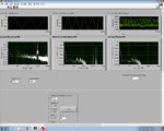
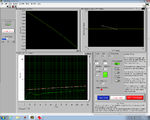
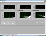
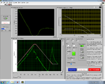
| − | | <center> | + | | <center> Lock-In GUI screens EARLY in a melting/annealing cycle </center> |
| | | | ||
|- | |- | ||
| − | | [[Image:DNAMeltingLabViewLeftEarly.png|150 px|thumb|center| | + | | [[Image:DNAMeltingLabViewLeftEarly.png|150 px|thumb|center|GUI Raw Signals]] |
| − | | [[Image:DNAMeltingLabViewCenterEarly.png|150 px|thumb|center| | + | | [[Image:DNAMeltingLabViewCenterEarly.png|150 px|thumb|center|GUI Lock-in]] |
| − | | [[Image:DNAMeltingLabViewRightEarly.png|150 px|thumb|center| | + | | [[Image:DNAMeltingLabViewRightEarly.png|150 px|thumb|center|GUI Control Panel]] |
|- | |- | ||
| | | | ||
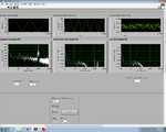
| − | | <center> | + | | <center> Lock-In GUI screens LATE in a melting/annealing cycle (notice large bleaching) </center> |
| | | | ||
|- | |- | ||
| − | | [[Image:DNAMeltingLabViewLeftLate.png|150 px|thumb|center| | + | | [[Image:DNAMeltingLabViewLeftLate.png|150 px|thumb|center|GUI Raw Signals]] |
| − | | [[Image:DNAMeltingLabViewCenterLate.png|150 px|thumb|center| | + | | [[Image:DNAMeltingLabViewCenterLate.png|150 px|thumb|center|GUI Lock-in]] |
| − | | [[Image:DNAMeltingLabViewRightLate.png|150 px|thumb|center| | + | | [[Image:DNAMeltingLabViewRightLate.png|150 px|thumb|center|GUI Control Panel]] |
|} | |} | ||
| Line 184: | Line 178: | ||
Your task is two-fold: 1) Produce three (3) precision melting curves for each of the three known samples and calibrate your instrument by comparing them to known standards or simulated results, and 2) produce three (3) precision melting curves for the unknown sample and determine its identity. | Your task is two-fold: 1) Produce three (3) precision melting curves for each of the three known samples and calibrate your instrument by comparing them to known standards or simulated results, and 2) produce three (3) precision melting curves for the unknown sample and determine its identity. | ||
| − | To begin, open the <code> | + | To begin, open the <code>DNALockIn.m</code> Matlab GUI and follow the instructions there. Take some time to get to know your new instrument using the fluorescein and old dsDNA samples provided. Debug your instrument so that you can reliably produce a precision melting curve. Maximize SNR using the new procedure described below. Work with a TA or Instructor to verify that your instrument is in peak operating condition. Be sure that your analysis scripts are also in peak operating condition. Then and only then, work through the final experimental steps described below. |
====Final experiment steps==== | ====Final experiment steps==== | ||
#Find your group listed on the white board in lab and retrieve your group's sample set from the sample box for this semester, located in the refrigerator. | #Find your group listed on the white board in lab and retrieve your group's sample set from the sample box for this semester, located in the refrigerator. | ||
| − | #Prepare a sample as described previously and place | + | #Prepare a sample as described previously and place the vial in your heating block. |
| − | #Use the | + | #Use the GUI as instructed there to record RTD and photodiode output during heating and cooling. |
#Time allowing, repeat the last steps two (2) more times for each of your known sample types, using a new 500 uL shot of sample for each run, for a total of up to three (3) curves per sample. Save the data for each run. The three runs (time allowing) per sample type will allow you to judge the consistency of your execution. In particular, the temperature transfer function between the block and the sample can be variable if sample loading and setup are inconsistent. | #Time allowing, repeat the last steps two (2) more times for each of your known sample types, using a new 500 uL shot of sample for each run, for a total of up to three (3) curves per sample. Save the data for each run. The three runs (time allowing) per sample type will allow you to judge the consistency of your execution. In particular, the temperature transfer function between the block and the sample can be variable if sample loading and setup are inconsistent. | ||
#Finally, prepare samples and record three (3) melting curves for your unknown sample type. For the unknown, you should be sure to have three (3) runs. | #Finally, prepare samples and record three (3) melting curves for your unknown sample type. For the unknown, you should be sure to have three (3) runs. | ||
| Line 197: | Line 191: | ||
===Measuring signal to noise=== | ===Measuring signal to noise=== | ||
| − | Carry out a test of the signal to noise ratio (SNR) of your instrument by inserting a fresh sample of dsDNA and then running the | + | Carry out a test of the signal to noise ratio (SNR) of your instrument by inserting a fresh sample of dsDNA and then running the GUI, <code>SNRLockIn.m</code>, provided under the <code>CourseMaterials/Labs/DNAMelting</code> folder. Run this GUI with your desired operating conditions until the strip chart at the top of the screen is full of good data, and click "Save Data" to record this data to disk. Next, open Matlab, load your file into an array and run its transpose through the <code>SToNCalculator.m</code> function provided, using no semicolon after the function name. This function will output graphical representations of your data along with your calculated SNR numbers. Your instrument will be rated based on it's "Adjusted SNR." |
==Opportunities for further development== | ==Opportunities for further development== | ||
For those so-inclined, there is much fertile ground for further improvement of both the instrument and our understanding of the physical processes involved. We welcome your interest in pursuing such improvements. Some possibilities are listed here. | For those so-inclined, there is much fertile ground for further improvement of both the instrument and our understanding of the physical processes involved. We welcome your interest in pursuing such improvements. Some possibilities are listed here. | ||
| − | *There is another method for controlling the heating profile of your DNA sample. It so happens that the heater/cooler board has been designed as a "shield" for an Arduino controller board. An initial version of software for that purpose has been tested and debugged. One next step that could be to integrate the Arduino controller into the over-all | + | *There is another method for controlling the heating profile of your DNA sample. It so happens that the heater/cooler board has been designed as a "shield" for an Arduino controller board. An initial version of software for that purpose has been tested and debugged. One next step that could be to integrate the Arduino controller into the over-all Lock-In GUI. See us if you are interested. |
*You will fit a multi-parameter model to your data. One primary weakness in our implementation of such a model at this time involves the convective heat loss term in the transfer function of the heating lag model between the block and the sample. We have some ideas to address this. If you do also, or would like to hear more, please see us. | *You will fit a multi-parameter model to your data. One primary weakness in our implementation of such a model at this time involves the convective heat loss term in the transfer function of the heating lag model between the block and the sample. We have some ideas to address this. If you do also, or would like to hear more, please see us. | ||
| − | *Also, to do a DNA melting curve properly, one must heat (or cool) the sample extremely slowly. If we tried this with our current approach the sample would be far too bleached by the end. One method to address this would be to revise the | + | *Also, to do a DNA melting curve properly, one must heat (or cool) the sample extremely slowly. If we tried this with our current approach the sample would be far too bleached by the end. One method to address this would be to revise the Lock-In GUI so that the LED turns only briefly, and only after temperatures have stabilized to eliminate the lag between block and sample. If you are interested in tackling this, please see one of us. |
*Next, we do not believe that we have a fully-developed bleaching correction for this experiment. You may agree after trying your hand at this correction. If you would like to investigate further, please see one of us. | *Next, we do not believe that we have a fully-developed bleaching correction for this experiment. You may agree after trying your hand at this correction. If you would like to investigate further, please see one of us. | ||
*Any and all other ideas for improvement will also be given fair review! | *Any and all other ideas for improvement will also be given fair review! | ||
| Line 223: | Line 217: | ||
#[http://www.national.com/ds/LF/LF411.pdf LF411 Op-amp datasheet] | #[http://www.national.com/ds/LF/LF411.pdf LF411 Op-amp datasheet] | ||
#[http://www.national.com/ds/LM/LM741.pdf LM741 Op-amp datasheet] | #[http://www.national.com/ds/LM/LM741.pdf LM741 Op-amp datasheet] | ||
| − | |||
Revision as of 16:46, 15 October 2013
In part 1 of the DNA Melting Lab, you constructed a simple temperature cycler/fluorometer. The instrument has several shortcomings, including an inability to control the heating rate and susceptibility to noise.
In part 2 you will improve your instrument and data analysis by implementing a number of hardware and software changes. The goal is to make a good measurement. There is plenty of unexplored territory. Do something novel. Think of the lab manual as a set of suggestions. Do whatever makes your instrument better. Go crazy.
Recommended changes include:
- Optimizing the optical system.
- Adding a heating/cooling controller to your system.
- Revising your LED driver and photodiode amplifier circuits to support lock-in signal detection.
- Downloading and using a Matlab GUI that implements the software portions of temperature control and lock-in detection.
- Refining data analysis by modeling important system behaviors such as photobleaching and temperature lag.
Lock-in signal detection
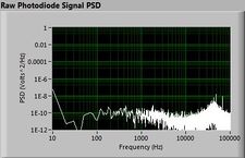
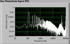
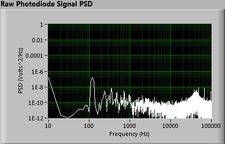
Lock-in signal detection provides some immunity to the very noisy lab environment. The plots below show typical Power Spectral Density measurements of noise in the 20.309 lab, a mix of optical and electronic noise. Fluorescent lighting creates a very strong technical noise at 120 Hz and harmonics. The lock-in technique moves the signal spectrum from the riotous low frequency realm to a calmer range of frequencies within the laboratory background noise spectrum. Noise in lab the may change without notice, so it may be useful to measure the noise spectrum before settling on a modulation frequency for your lock-in amplifier.
| |
||
| |
|
|
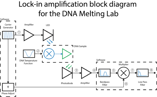
A block diagram of the lock-in scheme is shown below. Implementing lock-in detection requires the ability to modulate the LED output with a carrier frequency and signal processing (in software) to recover the baseband signal. To support these functions, the LED circuit must be modified to include a feedback brightness controller. In addition, the photodiode amplifier must be modified to accommodate the change in signal frequency range. In the GUI, you will need to choose the LED drive and frequency parameters to support your design.
LED modulation
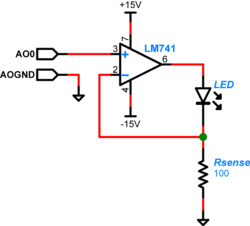
The LED used in this lab can operate up to 30mA of current when driven to its full range. In Part 1 of the lab you had used roughly the full 30 mA. For Part 2 you will drive the LED with an op-amp which will limit the current to about 10 mA. LED radiant flux — your excitation light — is proportional to current, so we will implement a controlled current source and direct it through the LED to provide a stable sample excitation.
To implement the current source to drive your LED, you will use an LM741 op-amp[1], with the output connected to the LED and a current sensing feedback resistor. Out feedback setup means we are controlling the total current through the LED. The feedback voltage is directly proportional to the resistor current and because of our choice of resistor value, the current through the LED is proportional to the voltage applied to the op-amp positive input by the DAQ. (Remember the golden rules.) So we are easily able to control the current through the LED, and likewise able to control the excitation light delivered to our dsDNA specimen.
Adjust photodiode amplifier gain and add high-pass filter
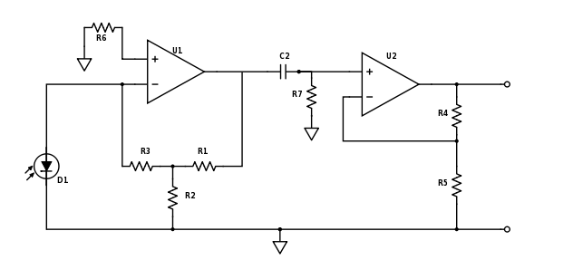
For Part 2 of the lab you will want to make some adjustments to your amplifier circuit. Principle among these are the adjustment of your low pass filter on the first stage and the addition of a high pass filter between stages. In Part 1, you were amplifying an essentially constant signal, aside from it's slow variation as the dsDNA denatured. Thus your low-pass filter in stage one was most likely tuned to remove noise at 60 Hz and above. In Part 2, the LED excitation light is modulated at a frequency much greater than 60 Hz and therefore the fluorescent emission from the SYBR Green is also modulated. You need to modify this low-pass filter to allow the modulated signal to get through the first stage.
Next, since the 60 Hz, 1/f, fluorescent light switching and other noise sources are likely lower than your LED modulation carrier frequency, you will want to insert a high-pass filter as shown in the updated schematic below. Think about the frequencies of the noise sources and your carrier frequency and choose an appropriate filter cutoff frequency.
Also be sure to re-evaluate the way in which you have gain distributed between the two stages. Now that the op-amps are responding to higher frequency signals, additional non-ideal characteristics may come into play. Among these is the fact that the op-amps can only slew their output voltages at a certain rate. Because this limited slew-rate limits the peak-to-peak voltage that can be achieved over small time scales, the maximum gain that can be achieved will likewise be limited. Review the datasheet for your LF411 op-amps, dig around online or in the course reading materials, talk to an Instructor or TA, and research two particular specifications: the slew rate and the "unity gain bandwidth" or the "gain-bandwidth product." Slew rate is directly applicable to both your first-stage transimpedence amplifier topology and your second-stage non-inverting topology. The gain-bandwidth product is an easier to use summary specification provided by the manufacturers, but it is only applicable to the op-amp's use in the typical non-inverting or "voltage-in voltage-out" inverting topolgy.
Add heater controller board
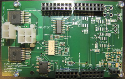
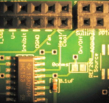
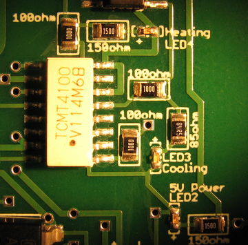
In order to control a slow ramp up and ramp down in block and sample temperature, the pulse width modulator (PWM) technique has been implemented on the heater/cooler printed circuit board (PCB) that is provided for you. Once the correct connections have been made, you will be able to control your block temperature using the Matlab GUI with minimal input on your part. It is not required that you learn the details of the heater/cooler controller design and operation, but if you want to know more, please talk to an Instructor or TA.
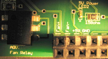
All points of connection are labeled on the PCB. Using the reference images above, make connections between your PCB and your DAQ cable (as described in the next section), and also your fan. The connection to the fan itself is self-explanatory, and is labeled as "Fan+" for the red wire and "Fan-" for the black wire.
Next, connect your TEC and the computer power supply for the TEC and fan. Do not yet switch on the Diablotek computer power supply. Connect your TEC to the 2-pin Molex male connector on the left of the board using a Part 2 (red/black wires) female connector provided on the counter in the same box as the Part 1 connector (Black/White wires). Connect the free end of the new TEC wires to your TEC stack using wire nuts as before. If your TEC is installed correctly, connect red-to-red and black-to-black. If it is upside down, reverse the connections. Now verify that the Diablotek computer power supply is not switched on. Then connect the the 4-pin connector from the Diablotek that IS NOT labeled for Part 1 to the "Diablotek" 4-pin connector labeled on the PCB. These 2-pin and 4-pin connectors are all white, in contrast to the one black connector that you used for Part 1.
Do not yet switch on the Diablotek.
Finally, several status LEDs are provided on the PCB. A green LED will tell you whether the logic circuits are receiving 5 V power. A red LED will indicate that you are sending a heating signal. And a blue LED will indicate that you are sending a cooling signal. These LEDs do not indicate whether the TEC is actually receiving power from the Diablotek. They only indicate that status of the controller logic.
Update your PC data acquisition system
Update the DAQ connections
In the DAQ connections inset above, the "Fan" connection is a 0 or 5 V signal from the DAQ, controlled by the Lock-In GUI. The "Heat/Cool" connection is a 0 or 5 V signal, also sent by the DAQ and controlled by the GUI, that tells the heater/cooler logic circuits to either heat (high, 5 V) or cool (low, 0 V). The DGND slot next to both the Fan and Heat/Cool connections should be connected to the digital ground of the DAQ, which is provide using the bare wire from your DAQ connector, as described in the handout.
Next, the "On/Off" connection also accepts a 0 or 5 V signal from the DAQ. However this signal is provided a square wave of varying duty cycle. This approach forms the heart of PWM power control. When the signal is high, the power switches in the large BTN7930 half-bridge chips are configured to allow current to flow through the TEC. The Heat/Cool signal controls the direction of power flow as noted above. When the On/Off signal is low, no power flows through the switches in either direction, when it is high, power will flow. A control loop inside the Lock-In GUI implements a Proportional-Integral-Derivative (PID) controller to set both the On/Off pulse widths and the Heat/Cool signal level in such a way as to maintain a desired temperature, or follow a desired temperature profile in time. The frequency of this duty cycle is pre-set at 10 Hz so that it's overtones do not interfere with the typical 10 kHz LED modulation frequency of your lock-in amplifier. If you choose a different LED modulation frequency, you may want to adjust the PWM frequency as well. The two half-bridge chips, connected and controlled as they are here, form what is called an H-bridge. If you want to know more, please ask an Instructor or TA.
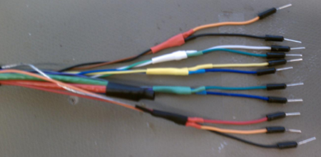
| Signal Name | Signal Location | Ground Location | Pin wire color |
|---|---|---|---|
| DAQ Inputs | |||
| RTD | AI0+ | AI0- | +Orange / -Black |
| Photodiode | AI1+ | AI1- | +Green / -White |
| DAQ Outputs | |||
| Fan | P1.1 | N/A | Orange |
| Heat/Cool | P1.0 | N/A | Red |
| Digital GND | DGND | N/A | Black (bundled with Red/Orange) |
| Heater/Cooler On/Off | +AO1 | AOGND | +Green / -Blue or -Black |
| LED Modulation Carrier | +AO0 | AOGND | +Yellow or +White / -Blue |
Recall that the DAQ connections and cable wire colors are also summarized in a memo. NOTE: the polarity of the photodiode inputs has been reversed in this lab manual, in comparison to the first version of the DAQ connector memo, to address the cross-talk issue that we recently discovered in the DAQ.
Update and test the Matlab GUI
The lock-in GUI is DNALockIn.m, provided for you on the course share in the CourseMaterials/Labs/DNAMelting folder. Be sure to make your own copy and adjust the parameters of the RTD temperature calculations as necessary. Follow the instructions in the GUI to run an experiment.
However, before you run any experiments, verify that you have connected the PCB board to the DAQ and TEC power supply appropriately. First open the GUI in Matlab and start it by clicking the green "Run" arrow. Next turn on your +/- 15 V power supply and toggle the LED button to verify that your LED circuit works. If not, make a note of it to come back to it later.
Now turn on the Diablotek TEC power supply. Your fan should start at the same time. Any time the TEC power supply is on, the fan will turn on automatically when you first start-up this GUI, it will turn off when you start to heat, and it will turn back on when either the temperature profile enters the cool-down phase or when you click on the cool-down override button in the GUI. The fan is necessary to help your heat sink dissipate the waste heat that is pumped from the top side of the TEC stack during cooling operations.
Finally, click "START" to start a heating cycle. The fan should turn off, the red heating status LED should light up, and the temperature of your heating block should start to respond. Be sure that your TEC power supply is on for this test. You may want to adjust the heating profile for debugging purposes.
If any of the steps above do not give the expected outcome: Investigate, hypothesize, make an adjustment, and start again at the DAQ connections.
| |
||
| |
||
Part 2 Experimental procedure
Most of the experimental procedure for part 2 is identical to that of part 1. All of the Safety and Environmental precautions listed there also apply here. In part 2 we will give you three known dsDNA samples, and one unknown sample. The three know samples will vary in either number of base pairs in the oligos, buffer ionic strength, or the degree of match between the two oligos in solution. The unknown sample will be one of your know samples.
Your task is two-fold: 1) Produce three (3) precision melting curves for each of the three known samples and calibrate your instrument by comparing them to known standards or simulated results, and 2) produce three (3) precision melting curves for the unknown sample and determine its identity.
To begin, open the DNALockIn.m Matlab GUI and follow the instructions there. Take some time to get to know your new instrument using the fluorescein and old dsDNA samples provided. Debug your instrument so that you can reliably produce a precision melting curve. Maximize SNR using the new procedure described below. Work with a TA or Instructor to verify that your instrument is in peak operating condition. Be sure that your analysis scripts are also in peak operating condition. Then and only then, work through the final experimental steps described below.
Final experiment steps
- Find your group listed on the white board in lab and retrieve your group's sample set from the sample box for this semester, located in the refrigerator.
- Prepare a sample as described previously and place the vial in your heating block.
- Use the GUI as instructed there to record RTD and photodiode output during heating and cooling.
- Time allowing, repeat the last steps two (2) more times for each of your known sample types, using a new 500 uL shot of sample for each run, for a total of up to three (3) curves per sample. Save the data for each run. The three runs (time allowing) per sample type will allow you to judge the consistency of your execution. In particular, the temperature transfer function between the block and the sample can be variable if sample loading and setup are inconsistent.
- Finally, prepare samples and record three (3) melting curves for your unknown sample type. For the unknown, you should be sure to have three (3) runs.
| |
IMMEDIATELY return any DNA to the refrigerator unless it is being analyzed in your instrument. |
Measuring signal to noise
Carry out a test of the signal to noise ratio (SNR) of your instrument by inserting a fresh sample of dsDNA and then running the GUI, SNRLockIn.m, provided under the CourseMaterials/Labs/DNAMelting folder. Run this GUI with your desired operating conditions until the strip chart at the top of the screen is full of good data, and click "Save Data" to record this data to disk. Next, open Matlab, load your file into an array and run its transpose through the SToNCalculator.m function provided, using no semicolon after the function name. This function will output graphical representations of your data along with your calculated SNR numbers. Your instrument will be rated based on it's "Adjusted SNR."
Opportunities for further development
For those so-inclined, there is much fertile ground for further improvement of both the instrument and our understanding of the physical processes involved. We welcome your interest in pursuing such improvements. Some possibilities are listed here.
- There is another method for controlling the heating profile of your DNA sample. It so happens that the heater/cooler board has been designed as a "shield" for an Arduino controller board. An initial version of software for that purpose has been tested and debugged. One next step that could be to integrate the Arduino controller into the over-all Lock-In GUI. See us if you are interested.
- You will fit a multi-parameter model to your data. One primary weakness in our implementation of such a model at this time involves the convective heat loss term in the transfer function of the heating lag model between the block and the sample. We have some ideas to address this. If you do also, or would like to hear more, please see us.
- Also, to do a DNA melting curve properly, one must heat (or cool) the sample extremely slowly. If we tried this with our current approach the sample would be far too bleached by the end. One method to address this would be to revise the Lock-In GUI so that the LED turns only briefly, and only after temperatures have stabilized to eliminate the lag between block and sample. If you are interested in tackling this, please see one of us.
- Next, we do not believe that we have a fully-developed bleaching correction for this experiment. You may agree after trying your hand at this correction. If you would like to investigate further, please see one of us.
- Any and all other ideas for improvement will also be given fair review!
Lab manual sections
- Lab Manual:Measuring DNA Melting Curves
- DNA Melting: Simulating DNA Melting - Basics
- DNA Melting Part 1: Measuring Temperature and Fluorescence
- DNA Melting Report Requirements for Part 1
- DNA Melting Part 2: Lock-in Amplifier and Temperature Control
- DNA Melting Report Requirements for Part 2

