Difference between revisions of "DNA Melting Part 2: Lock-in Amplifier and Temperature Control"
Steven Nagle (Talk | contribs) (→Add heater controller board) |
Juliesutton (Talk | contribs) (→Test the system) |
||
| (295 intermediate revisions by 8 users not shown) | |||
| Line 3: | Line 3: | ||
{{Template:20.309}} | {{Template:20.309}} | ||
| − | + | ==Overview== | |
| + | In part 2 of the DNA Melting Lab you will make changes to your DNA melter that will improve the quality of the melting curves you generate. Two of the most important improvements are adding lock-in detection to reduce the effects of optical noise and a temperature controller to enable control of the sample heating and cooling rates. You will also use a computer model to compensate for the difference in temperature between the heating block and sample, photobleaching, and thermal quenching of the fluorescent dye. | ||
| + | Use the fluorescein and "beater" DNA samples available in the lab to test and debug your system. Continue refining your instrument until you are satisfied with the results. Please use DNA samples judiciously (even the "beater" DNA). Keep DNA sample samples out of the light when you are not taking data to reduce photobleaching. | ||
| − | == | + | ==Electronic circuit changes for lock-in detection== |
| − | + | [[Image:DNA_Lock-in_Block_Diagram_20130725.png|right|thumb|Block diagram of lock-in amplifier for DNA melting]] | |
| + | There are two important changes needed to implement lock-in detection on your DNA melter — making the LED intensity vary sinusoidally, and modifying the photodiode amplifier to operate over a different range of frequencies. In part 1 of the lab, the optical signal consisted of very low frequencies. Multiplying the signal by a cosine moves the frequency range of interest much higher. You will have to change your amplifier circuit to handle the higher frequencies. | ||
| − | + | You will use an op-amp circuit to enable modulation of the LED. Modulating the LED will allow you to place the optical signal generated by the fluorescent dye in a low-noise area of the frequency spectrum. Recovering the original signal requires multiplying by a cosine of the same frequency and low-pass filtering. The multiplication and filtering is done in software. | |
| − | + | ||
| − | + | ===Build an LED driver=== | |
| + | [[Image:LED_Op-amp_Drive_Schematic.png|thumb|right|LED driver circuit]] | ||
| − | + | In order to take advantage of the lock-in technique to reduce noise from other photonic sources, the illumination from the blue LED has to be modulated with a cosine waveform. You will use an op amp to implement a circuit that will vary the current through the LED in proportion to the applied voltage. Software controlling the DAQ system will generate a cosine voltage waveform (typically at 10kHz) that you can use to drive the LED circuit. Remember that the LED current must be positive, so the software will also allow you to add a DC offset to the cosine waveform and keep the total voltage greater than zero. (For example, choose a cosine amplitude of 1 V and an of offset 1.2 V.) | |
| − | + | A schematic diagram of the LED driver circuit is shown on the right. Note that it uses a different model of op amp than the ones in your transimpedance amplifier: an LM741. Choose the resistor ''Rsense'' to limit the current through the LED (too much current will wreck it). The smoke will stay inside the LED as long as you keep the current below 30mA. | |
| − | + | ====Parts==== | |
| + | * LM741 op-amp from the Electronics Drawer | ||
| + | * Current feedback resistor | ||
| − | === | + | ===Part 2 photodiode amplifier=== |
| − | + | [[Image:Part2_TransimpedanceAmplifier.jpg|thumb|center|450px|Part 2 photodiode amplifier.]] | |
| + | In part 1 of the lab, you used a capacitor in the first gain stage of the photodiode amplifier to implement a low-pass filter. Modulating the LED will move the signal to a much higher frequency. So rip that sucker off — now your amplifier needs to work on a signal that is changing much more quickly. | ||
| − | + | Photonic noise at low frequencies is very large — frequently much larger than the signal from the fluorescent dye. For this reason, the part 2 amplifier includes a high-pass filter that removes much of the low-frequency junk before it gets amplified by the second stage. Pick values for C2 and R7 so that the cutoff frequency gets rid of as much of the low-frequency noise as possible while still allowing the ~10kHz modulated DNA signal to pass. | |
| − | + | For a real op-amp the golden rules are only approximately true, and small amounts of current can flow into the input terminals. The effects of this current are minimized when the input impedance of the + and - terminals are balanced. Assuming R2 < R1 and R3, choosing R6 ≈ R3 should give you the desired results. | |
| − | + | After you make these changes, double check that everything is still working well. You may need to update the gains of one or both of your amplifier stages to work best with the lower signal level and increased frequency. | |
| − | + | ||
| − | + | ===Minimizing electronic noise=== | |
| + | You probably noticed a good amount of noise in the signals from your DNA melter in part 1. Fundamental noise sources such as shot noise and dark current noise certainly had an effect, but it is likely that technical sources of electronic and optical noise were a much larger problem. This section explains some of the steps you can take to reduce the susceptibility of your instrument to technical noise sources. | ||
| − | + | <figure id="fig:SourcesOfElectronicNoise">[[File:Sources of electronic noise.png|thumb|right|<caption>Sources of electronic noise include common mode noise, electromagnetic coupling, noise conducted through power lines, and Johnson noise.</caption>]]</figure> | |
| + | ====Electronic noise==== | ||
| + | <xr id="fig:SourcesOfElectronicNoise" /> shows four ways that electronic noise can enter circuits. | ||
| − | + | * Electromagnetic fields induce currents in the wires that make up your circuit. There are many sources of electromagnetic fields that can interfere with your circuit: power lines, other pieces of electronic equipment, electrostatic discharges, and radio signals. | |
| − | + | * Noise from other pieces of equipment can be conducted through power lines. | |
| − | + | * Real wires and connectors have nonzero resistance. Current flowing through a common ground wire causes the ground potential to shift. | |
| + | * Random currents arise in conductors at maintained at nonzero temperatures due to the thermal energy of the electrons. This phenomenon is called Johnson noise. The magnitude of random voltages gets larger as the resistance of the conductor increases. | ||
| − | + | Here are some suggestions for things you can do to reduce electronic noise in your DNA circuit: | |
| + | <br /><br /> | ||
| + | <gallery widths=216px caption="Ways to minimize electronic noise:"> | ||
| + | File:Neat wiring.jpg|Keep the component layout compact. Make ground connections close together. Keep your wiring short and neat. | ||
| + | File:Bypass caps.jpg|Use power supply bypass capacitors with C > 1 μF. Capacitors connected across the power supply lines, placed close to powered components, will reduce noise in the power supply line. | ||
| + | File:Multiple ground wires.jpg|Connect parallel wires to the power supplies. Multiple conductors in parallel will reduce parasitic resistance, which in turn will decrease voltage fluctuations due to common mode currents. | ||
| + | File:Separate LED from amp.jpg|Separate high-current portions of the circuit like the LED driver from sensitive components like the transimpedance amplifier. | ||
| + | File:RTD capacitor.JPG|Use a capacitor to eliminate high-frequency noise from the temperature signal. | ||
| + | </gallery> | ||
| − | + | ==Temperature control== | |
| + | A software control loop implements a Proportional-Integral-Derivative (PID) controller in order to maintain the sample block at a desired temperature. Digital signals control high-current switches (called an H-bridge) to make the TECs heat, cool, or remain inactive. Temperature control is effected by setting the duty cycle of these three functions. A fan carries away excess heat. | ||
| − | + | ===Add a temperature controller board=== | |
| + | The temperature controller includes of a printed circuit board (PCB) that can apply current to the TEC in either direction, which in turn causes heat flow in or out of the sample block. The board is controlled by digital signals from the DAQ that are generated in the part-2 version of the DNA melter software. | ||
| − | + | Three status LEDs are provided on the PCB. A lighted green LED will confirms power applied. A red LED will indicates sample heating mode; blue means cooling. | |
| − | + | Important: if you see a blue or red light when you are not running an experiment, immediately turn off the Diablotek power supply. Leaving the system stuck in heating or cooling mode for a long time will result in runaway temperatures that will likely destroy a TEC. Don't do that — fixing the problem requires a lengthy and mess removal and replacement process. | |
| − | + | ====Parts==== | |
| + | Gather the following components: | ||
| + | <gallery widths=216px> | ||
| + | File:DNA_HeaterPCB_v5.PNG|1 PCB heater/cooler board from the Center Cabinets or the East Cabinets. | ||
| + | File:RedBlack Molex Connector.jpg|1 red/black connector cable to hook up the Peltier device (TEC) to the heater/cooler board (from the East Cabinets). | ||
| − | + | </gallery> | |
| − | === | + | ====Assembly==== |
| − | + | Points of connection are labeled on the PCB and described in the table and figure below. Refer to both in the instructions that follow. | |
| − | [[Image: | + | # Place the PCB in the pre-drilled holes on the sheet metal support bracket. |
| − | + | #* If the nylon "feet" are missing, add them now. They are in the DNA Melting drawer at the right of the Wet Bench. | |
| − | + | # Disconnect the yellow/white cable between the power supply and the TEC stack. | |
| − | | | + | # Connect the red/black connector cable to the TEC stack. |
| + | #* Join the red wire to the red lead of the top TEC and the black wire to the black lead on the bottom TEC using wire nuts. | ||
| + | #* Plug the white Molex connector at the other end of the red/black cable to its mate on the PCB. | ||
| + | # Turn off the Diablotek power supply. | ||
| + | # Connect the Diablotek and check power [[Image:PCB connectors 2.JPG|thumb|right|Connect the fan to the PCB]] | ||
| + | #* Connect the Diablotek 4-pin/3-color power supply connector to the PCB. (NOTE: this is different from the connector that you used in Part 1. The connector is white instead of black.) | ||
| + | #* Quickly cycle the Diablotek power to confirm a green power status light in the upper right corner of the PCB. | ||
| + | #* Confirm that the Diablotek is off. | ||
| + | # Connect the fan itself to the Fan +/- connections at the bottom of the PCB (red to +, black to -, innermost row. See figure). | ||
| + | |||
| + | ===Update your PC data acquisition system=== | ||
| + | You will need to route several additional signals from the DAQ to your DNA melter to control the LED modulation and temperature control board. | ||
| + | |||
| + | The DAQ connections and cable wire colors are summarized in the table below, and [http://dl.dropbox.com/u/12957607/DAQ_Cable_Assembly_for_DNA_melting_lab.pdf the document]. | ||
| + | |||
| + | {| class="wikitable" | ||
| + | |- | ||
| + | ! Signal Name | ||
| + | ! Signal Location | ||
| + | ! Ground Location | ||
| + | ! Pin wire color | ||
| + | |- | ||
| + | ! DAQ Inputs | ||
| + | |- | ||
| + | ! RTD | ||
| + | | AI0+ | ||
| + | | AI0- | ||
| + | | +Orange / -Black (lone pair) | ||
| + | |- | ||
| + | ! Photodiode | ||
| + | | AI1+ | ||
| + | | AI1- | ||
| + | | +Green / -White | ||
| + | |- | ||
| + | ! DAQ Outputs | ||
| + | |- | ||
| + | ! Fan | ||
| + | | P1.1 | ||
| + | | N/A | ||
| + | | Orange | ||
| + | |- | ||
| + | ! Heat/Cool | ||
| + | | P1.0 | ||
| + | | N/A | ||
| + | | Red | ||
| + | |- | ||
| + | ! Digital GND | ||
| + | | DGND | ||
| + | | N/A | ||
| + | | Black (bundled with Red/Orange) | ||
| + | |- | ||
| + | ! Heater/Cooler On/Off | ||
| + | | CTR0 | ||
| + | | DGND/AOGND | ||
| + | | +Green / -Blue or -Black | ||
|- | |- | ||
| − | | | + | ! LED Modulation Carrier |
| − | | | + | | AO0 |
| + | | AOGND | ||
| + | | +Yellow or +White / -Blue | ||
|} | |} | ||
| − | + | ====Connect the DAQ cable to the control board==== | |
| + | |||
| + | [[Image:DAQ_Wire_Colors.png|thumb|right|DAQ Connection Cable]] | ||
| + | [[Image:PCB connectors 1.JPG|thumb|right|Connect the DAQ to the PCB]] | ||
| + | # Connect the orange Fan signal pin to the Fan signal header socket at the top of the PCB (innermost row). | ||
| + | # Connect the black digital GND signal pin to the marked DGND header socket at the top of the PCB (innermost row). | ||
| + | # Connect the red Heat/cool signal pin to the marked Heat/cool header socket at the top of the PCB (innermost row). | ||
| + | # Connect the green/blue or green/black Heater/cooler On/off signal pins to the marked header sockets at the top of the PCB (innermost row). | ||
| + | # If you have not already done so, connect the appropriate DAQ cables to the RTD and LED circuits on your breadboard. | ||
| − | |||
| − | + | ==Test the system== | |
| + | Data acquisition and control is done by the "Lockin DNA Melter GUI", provided for you on the lab computer desktop. Follow the instructions in the [[DNA Melting: Using the LockIn DNAMelter GUI|LockIn DNAMelter GUI wiki page]] to become familiar with the software. You may find it useful to review the block diagram again on the [[Understanding the lock-in amplifier]] wiki page. | ||
| − | + | Before you run any experiments, verify that you have connected the PCB board to the DAQ and TEC power supply appropriately. | |
| + | [[Image:GUILockInEarlyView.jpg|thumb|right|Early in melting cycle]] | ||
| + | [[Image:GUILockInLaterView.jpg|thumb|right|Late in melting cycle]] | ||
| − | + | # Run the <tt>LockInGUI</tt> in MATLAB. | |
| + | # Turn on your +/- 15V power supply. | ||
| + | # Toggle the LED button in the GUI to verify that your LED circuit works. If not, check your connections. | ||
| + | # Use a fluorescent sample (DNA or fluorescein) to test your optical path | ||
| + | #* With the fluorescent sample loaded, turn on the LED. | ||
| + | #* Remove the sample (or replace it with a vial filled with water) and you should see a change in the fluorescence signal. If not, debug. | ||
| + | # Turn on the Diablotek TEC power supply. | ||
| + | #* Your fan should start at the same time. Any time the TEC power supply is on, the fan will turn on automatically when you first start-up this GUI, it will turn off when you start to heat, and it will turn back on when either the temperature profile enters the cool-down phase or when you click on the cool-down override button in the GUI. The fan is necessary to help your heat sink dissipate the waste heat that is pumped from the top side of the TEC stack during cooling operations. | ||
| + | # Finally, click "START" to start a heating cycle. | ||
| + | #* The fan should turn off, the red heating status LED should light up, and the temperature of your heating block should start to respond. Be sure that your TEC power supply is on for this test. You may want to adjust the heating profile for debugging purposes. | ||
| + | Test,debug and improve your instrument until you are satisfied with the results. Fluorescein and "beater" DNA samples are available for debugging and bringup, but please use judiciously. To preserve your fresh DNA sample, quickly remove from the instrument and protect from light when not gathering data. It is wise to run several beater-DNA samples and process the data to ensure that your instrument is operating properly and reliably before moving on to your real samples. | ||
| − | + | ==Experimental procedure== | |
| − | + | ===Measure SNR=== | |
| − | + | Using a fresh DNA sample, and choosing the same operating conditions that you will use to collect your melting curve data, carry out a test of the signal to noise ratio (SNR). Launch the <code> SNR Lockin DNA Melter GUI</code>, collect data until the strip chart at the top of the screen is full of good data, then click "Save Data" to record this data to disk. Next, open Matlab, load your SNR output file into an array and run its transpose through the [[SToNCalculator.m]] function provided, using no semicolon after the function name: | |
| − | + | ||
| − | + | <code>snr = load ('snrFile.txt')'; | |
| − | + | StoNCalculator( snr, 'sampleName')</code> | |
| + | This function will output graphical representations of your data along with your calculated SNR numbers. Your instrument will be rated based on its "Adjusted SNR." | ||
| + | |||
| + | ===Identify unknown sample=== | ||
| + | You will receive 1.5 mL each of four samples. Three of the samples will be identified by their sequence, salt ion concentration, and degree of complementarity (see these [[DNA_Melting:_DNA_Sequences]]). The fourth sample matches one of the three identified samples. You will not be told which one. | ||
| + | |||
| + | * Acquire melting curves for the known and unknown samples. | ||
| + | ** You may want to run some or all of the samples more than once to provide more confidence in your result. | ||
| + | * Identify the unknown sample and report your confidence in the result. | ||
| + | ** See [[Identifying the unknown DNA sample]] for some ideas on identifying the sample. | ||
| + | ** You may use a different statistical procedure, if you like. Be sure to document the procedure you used. | ||
| + | * Report a quantitative measure of your confidence in the identification. | ||
| + | |||
| + | ==Analysis== | ||
| + | We set out to measure the fraction of dsDNA versus temperature. As discussed in lecture, factors like photobleaching, thermal quenching, and the difference between the block and sample temperature distorted the measurement in various ways. For the final report, you will carefully analyze your data using a mechanistic model to factor out the melting dynamics from the shortcomings of the measurement technique. | ||
| + | |||
| + | In an ideal world, you would have your analysis code written before the data is collected. In the real world, data collection involves a lot of waiting around, and it might be a good use of your time to work on the analysis code and collect data in parallel. In that case, it is still important to ensure that your data makes sense as it comes in. For example, is the trend in the melting temperature what you expected? … e.g. did longer oligos have a higher melting temperature than shorter ones? The following section provides a quick way to estimate melting temperatures from the raw data. | ||
| + | |||
| + | ===Estimating melting temperatures from raw data=== | ||
| + | [[Image:Delta Vf Delta theta versus theta.png|thumb|right| ∂''V<sub>f</sub>'' / ∂ ''T'' versus ''T'']] | ||
| + | A frequently-used, quick-and-dirty proxy for melting temperature is the peak value of the fluorescence voltage's derivative as a function of temperature. The peak of the derivative is the temperature at which the equilibrium is changing most rapidly. It's not exactly the same as the melting temperature, but it allows for quick comparison of results. | ||
| + | |||
| + | You can't just take the derivative of the raw signal. The raw data is not guaranteed to be a function at all. One way to take a good derivative is to combine the fluorescence voltage values that fall into a particular range of temperatures and then take the average of all those values — a process sometimes called ''binning'' or ''discretization''. Temperature bins of about a quarter of a degree work well. The code below demonstrates how to accomplish this in MATLAB. Because of the difference between the block and sample temperatures, it is best to do this for just the heating or melting portion of the curve. | ||
| + | |||
| + | Assuming the variables <code>temperature</code> and <code>fluorescence</code> are defined, the following Matlab code fragment below computes ΔF/ΔT for the heating portion of the curve. If your melting curves are very noisy, you may have to adjust the code. | ||
| + | |||
| + | <pre> | ||
| + | discretizationInterval = 0.25; | ||
| + | discreteTemperatureAxis = 20: discretizationInterval:100; % center value for each bin | ||
| + | discreteTemperaturBinEdges = [ discreteTemperatureAxis - discretizationInterval / 2, discreteTemperatureAxis(end) + discretizationInterval / 2 ]; | ||
| + | temperatureBinIndex = discretize( temperature, discreteTemperaturBinEdges ); | ||
| + | binnedFluorescence = accumarray( temperatureBinIndex', fluorescence', size( discreteTemperatureAxis' ), @mean )'; | ||
| + | badOnes = binnedFluorescence == 0; | ||
| + | discreteTemperatureAxis( badOnes ) = []; | ||
| + | binnedFluorescence( badOnes ) = []; | ||
| + | |||
| + | figure | ||
| + | subplot(211) | ||
| + | plot( discreteTemperatureAxis, binnedFluorescence ) | ||
| + | title( 'Average Fluorescence Voltage versus Temperature') | ||
| + | xlabel( 'T (^{\circ}C)' ) | ||
| + | ylabel( 'F (AU)' ) | ||
| + | |||
| + | dFluorescenceDTemperature = diff( binnedFluorescence ) ./ diff( discreteTemperatureAxis ); | ||
| + | derivativeAxis = mean( [ discreteTemperatureAxis(1:(end-1)); discreteTemperatureAxis(2:end) ] ); | ||
| + | |||
| + | subplot(212) | ||
| + | plot( derivativeAxis, dFluorescenceDTemperature); | ||
| + | title( 'Derivative of Fluorescence versus Temperature' ) | ||
| + | xlabel( 'T (^{\circ}C)' ) | ||
| + | ylabel( 'dF/dT' ) | ||
| + | </pre> | ||
| + | |||
| + | ===Using nonlinear regression to estimate parameters=== | ||
| + | |||
| + | The [[DNA Melting: Model function and parameter estimation by nonlinear regression]] wiki page will guide you in writing the model function used to estimate the relevant DNA melting parameters. | ||
| + | |||
| + | ==DNA Melting Report Requirements== | ||
| + | {{:DNA Melting Report Requirements for Part 2}} | ||
| + | |||
| + | ==Lab manual sections== | ||
| + | |||
| + | *[[Lab Manual:Measuring DNA Melting Curves]] | ||
*[[DNA Melting: Simulating DNA Melting - Basics]] | *[[DNA Melting: Simulating DNA Melting - Basics]] | ||
*[[DNA Melting Part 1: Measuring Temperature and Fluorescence]] | *[[DNA Melting Part 1: Measuring Temperature and Fluorescence]] | ||
*[[DNA Melting Report Requirements for Part 1]] | *[[DNA Melting Report Requirements for Part 1]] | ||
| − | |||
*[[DNA Melting Part 2: Lock-in Amplifier and Temperature Control]] | *[[DNA Melting Part 2: Lock-in Amplifier and Temperature Control]] | ||
*[[DNA Melting Report Requirements for Part 2]] | *[[DNA Melting Report Requirements for Part 2]] | ||
==References== | ==References== | ||
| − | <references /> | + | <references/> |
| + | |||
| + | ==Subset of datasheets== | ||
| + | (Many more can be found online or on the course share) | ||
| + | #[http://www.ni.com/pdf/manuals/371931f.pdf National Instruments USB-6212 user manual] | ||
| + | #[http://www.ni.com/pdf/manuals/370784d.pdf National Instruments USB-6341 user manual] | ||
| + | #[http://measurebiology.org/w/images/5/5b/Lf411-n.pdf LF411 Op-amp datasheet] | ||
| + | #[http://measurebiology.org/w/images/9/90/Lm741.pdf LM741 Op-amp datasheet] | ||
| − | + | {{Template:20.309 bottom}} | |
| − | + | ||
| − | + | ||
| − | + | ||
| − | + | ||
| − | + | ||
Latest revision as of 20:05, 7 November 2017

Overview
In part 2 of the DNA Melting Lab you will make changes to your DNA melter that will improve the quality of the melting curves you generate. Two of the most important improvements are adding lock-in detection to reduce the effects of optical noise and a temperature controller to enable control of the sample heating and cooling rates. You will also use a computer model to compensate for the difference in temperature between the heating block and sample, photobleaching, and thermal quenching of the fluorescent dye.
Use the fluorescein and "beater" DNA samples available in the lab to test and debug your system. Continue refining your instrument until you are satisfied with the results. Please use DNA samples judiciously (even the "beater" DNA). Keep DNA sample samples out of the light when you are not taking data to reduce photobleaching.
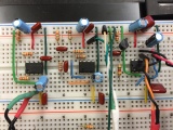
Electronic circuit changes for lock-in detection

There are two important changes needed to implement lock-in detection on your DNA melter — making the LED intensity vary sinusoidally, and modifying the photodiode amplifier to operate over a different range of frequencies. In part 1 of the lab, the optical signal consisted of very low frequencies. Multiplying the signal by a cosine moves the frequency range of interest much higher. You will have to change your amplifier circuit to handle the higher frequencies.
You will use an op-amp circuit to enable modulation of the LED. Modulating the LED will allow you to place the optical signal generated by the fluorescent dye in a low-noise area of the frequency spectrum. Recovering the original signal requires multiplying by a cosine of the same frequency and low-pass filtering. The multiplication and filtering is done in software.
Build an LED driver

In order to take advantage of the lock-in technique to reduce noise from other photonic sources, the illumination from the blue LED has to be modulated with a cosine waveform. You will use an op amp to implement a circuit that will vary the current through the LED in proportion to the applied voltage. Software controlling the DAQ system will generate a cosine voltage waveform (typically at 10kHz) that you can use to drive the LED circuit. Remember that the LED current must be positive, so the software will also allow you to add a DC offset to the cosine waveform and keep the total voltage greater than zero. (For example, choose a cosine amplitude of 1 V and an of offset 1.2 V.)
A schematic diagram of the LED driver circuit is shown on the right. Note that it uses a different model of op amp than the ones in your transimpedance amplifier: an LM741. Choose the resistor Rsense to limit the current through the LED (too much current will wreck it). The smoke will stay inside the LED as long as you keep the current below 30mA.
Parts
- LM741 op-amp from the Electronics Drawer
- Current feedback resistor
Part 2 photodiode amplifier
In part 1 of the lab, you used a capacitor in the first gain stage of the photodiode amplifier to implement a low-pass filter. Modulating the LED will move the signal to a much higher frequency. So rip that sucker off — now your amplifier needs to work on a signal that is changing much more quickly.
Photonic noise at low frequencies is very large — frequently much larger than the signal from the fluorescent dye. For this reason, the part 2 amplifier includes a high-pass filter that removes much of the low-frequency junk before it gets amplified by the second stage. Pick values for C2 and R7 so that the cutoff frequency gets rid of as much of the low-frequency noise as possible while still allowing the ~10kHz modulated DNA signal to pass.
For a real op-amp the golden rules are only approximately true, and small amounts of current can flow into the input terminals. The effects of this current are minimized when the input impedance of the + and - terminals are balanced. Assuming R2 < R1 and R3, choosing R6 ≈ R3 should give you the desired results.
After you make these changes, double check that everything is still working well. You may need to update the gains of one or both of your amplifier stages to work best with the lower signal level and increased frequency.
Minimizing electronic noise
You probably noticed a good amount of noise in the signals from your DNA melter in part 1. Fundamental noise sources such as shot noise and dark current noise certainly had an effect, but it is likely that technical sources of electronic and optical noise were a much larger problem. This section explains some of the steps you can take to reduce the susceptibility of your instrument to technical noise sources.

Electronic noise
Figure 1 shows four ways that electronic noise can enter circuits.
- Electromagnetic fields induce currents in the wires that make up your circuit. There are many sources of electromagnetic fields that can interfere with your circuit: power lines, other pieces of electronic equipment, electrostatic discharges, and radio signals.
- Noise from other pieces of equipment can be conducted through power lines.
- Real wires and connectors have nonzero resistance. Current flowing through a common ground wire causes the ground potential to shift.
- Random currents arise in conductors at maintained at nonzero temperatures due to the thermal energy of the electrons. This phenomenon is called Johnson noise. The magnitude of random voltages gets larger as the resistance of the conductor increases.
Here are some suggestions for things you can do to reduce electronic noise in your DNA circuit:
- Ways to minimize electronic noise:
Keep the component layout compact. Make ground connections close together. Keep your wiring short and neat.
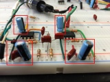
Use power supply bypass capacitors with C > 1 μF. Capacitors connected across the power supply lines, placed close to powered components, will reduce noise in the power supply line.
Connect parallel wires to the power supplies. Multiple conductors in parallel will reduce parasitic resistance, which in turn will decrease voltage fluctuations due to common mode currents.
Separate high-current portions of the circuit like the LED driver from sensitive components like the transimpedance amplifier.
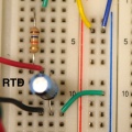
Use a capacitor to eliminate high-frequency noise from the temperature signal.


Temperature control
A software control loop implements a Proportional-Integral-Derivative (PID) controller in order to maintain the sample block at a desired temperature. Digital signals control high-current switches (called an H-bridge) to make the TECs heat, cool, or remain inactive. Temperature control is effected by setting the duty cycle of these three functions. A fan carries away excess heat.
Add a temperature controller board
The temperature controller includes of a printed circuit board (PCB) that can apply current to the TEC in either direction, which in turn causes heat flow in or out of the sample block. The board is controlled by digital signals from the DAQ that are generated in the part-2 version of the DNA melter software.
Three status LEDs are provided on the PCB. A lighted green LED will confirms power applied. A red LED will indicates sample heating mode; blue means cooling.
Important: if you see a blue or red light when you are not running an experiment, immediately turn off the Diablotek power supply. Leaving the system stuck in heating or cooling mode for a long time will result in runaway temperatures that will likely destroy a TEC. Don't do that — fixing the problem requires a lengthy and mess removal and replacement process.
Parts
Gather the following components:
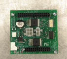
1 PCB heater/cooler board from the Center Cabinets or the East Cabinets.
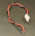
1 red/black connector cable to hook up the Peltier device (TEC) to the heater/cooler board (from the East Cabinets).


Assembly
Points of connection are labeled on the PCB and described in the table and figure below. Refer to both in the instructions that follow.
- Place the PCB in the pre-drilled holes on the sheet metal support bracket.
- If the nylon "feet" are missing, add them now. They are in the DNA Melting drawer at the right of the Wet Bench.
- Disconnect the yellow/white cable between the power supply and the TEC stack.
- Connect the red/black connector cable to the TEC stack.
- Join the red wire to the red lead of the top TEC and the black wire to the black lead on the bottom TEC using wire nuts.
- Plug the white Molex connector at the other end of the red/black cable to its mate on the PCB.
- Turn off the Diablotek power supply.
- Connect the Diablotek and check power
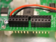 Connect the fan to the PCB
- Connect the Diablotek 4-pin/3-color power supply connector to the PCB. (NOTE: this is different from the connector that you used in Part 1. The connector is white instead of black.)
- Quickly cycle the Diablotek power to confirm a green power status light in the upper right corner of the PCB.
- Confirm that the Diablotek is off.
- Connect the fan itself to the Fan +/- connections at the bottom of the PCB (red to +, black to -, innermost row. See figure).

Update your PC data acquisition system
You will need to route several additional signals from the DAQ to your DNA melter to control the LED modulation and temperature control board.
The DAQ connections and cable wire colors are summarized in the table below, and the document.
| Signal Name | Signal Location | Ground Location | Pin wire color |
|---|---|---|---|
| DAQ Inputs | |||
| RTD | AI0+ | AI0- | +Orange / -Black (lone pair) |
| Photodiode | AI1+ | AI1- | +Green / -White |
| DAQ Outputs | |||
| Fan | P1.1 | N/A | Orange |
| Heat/Cool | P1.0 | N/A | Red |
| Digital GND | DGND | N/A | Black (bundled with Red/Orange) |
| Heater/Cooler On/Off | CTR0 | DGND/AOGND | +Green / -Blue or -Black |
| LED Modulation Carrier | AO0 | AOGND | +Yellow or +White / -Blue |
Connect the DAQ cable to the control board


- Connect the orange Fan signal pin to the Fan signal header socket at the top of the PCB (innermost row).
- Connect the black digital GND signal pin to the marked DGND header socket at the top of the PCB (innermost row).
- Connect the red Heat/cool signal pin to the marked Heat/cool header socket at the top of the PCB (innermost row).
- Connect the green/blue or green/black Heater/cooler On/off signal pins to the marked header sockets at the top of the PCB (innermost row).
- If you have not already done so, connect the appropriate DAQ cables to the RTD and LED circuits on your breadboard.
Test the system
Data acquisition and control is done by the "Lockin DNA Melter GUI", provided for you on the lab computer desktop. Follow the instructions in the LockIn DNAMelter GUI wiki page to become familiar with the software. You may find it useful to review the block diagram again on the Understanding the lock-in amplifier wiki page.
Before you run any experiments, verify that you have connected the PCB board to the DAQ and TEC power supply appropriately.


- Run the LockInGUI in MATLAB.
- Turn on your +/- 15V power supply.
- Toggle the LED button in the GUI to verify that your LED circuit works. If not, check your connections.
- Use a fluorescent sample (DNA or fluorescein) to test your optical path
- With the fluorescent sample loaded, turn on the LED.
- Remove the sample (or replace it with a vial filled with water) and you should see a change in the fluorescence signal. If not, debug.
- Turn on the Diablotek TEC power supply.
- Your fan should start at the same time. Any time the TEC power supply is on, the fan will turn on automatically when you first start-up this GUI, it will turn off when you start to heat, and it will turn back on when either the temperature profile enters the cool-down phase or when you click on the cool-down override button in the GUI. The fan is necessary to help your heat sink dissipate the waste heat that is pumped from the top side of the TEC stack during cooling operations.
- Finally, click "START" to start a heating cycle.
- The fan should turn off, the red heating status LED should light up, and the temperature of your heating block should start to respond. Be sure that your TEC power supply is on for this test. You may want to adjust the heating profile for debugging purposes.
Test,debug and improve your instrument until you are satisfied with the results. Fluorescein and "beater" DNA samples are available for debugging and bringup, but please use judiciously. To preserve your fresh DNA sample, quickly remove from the instrument and protect from light when not gathering data. It is wise to run several beater-DNA samples and process the data to ensure that your instrument is operating properly and reliably before moving on to your real samples.
Experimental procedure
Measure SNR
Using a fresh DNA sample, and choosing the same operating conditions that you will use to collect your melting curve data, carry out a test of the signal to noise ratio (SNR). Launch the SNR Lockin DNA Melter GUI, collect data until the strip chart at the top of the screen is full of good data, then click "Save Data" to record this data to disk. Next, open Matlab, load your SNR output file into an array and run its transpose through the SToNCalculator.m function provided, using no semicolon after the function name:
snr = load ('snrFile.txt')';
StoNCalculator( snr, 'sampleName')
This function will output graphical representations of your data along with your calculated SNR numbers. Your instrument will be rated based on its "Adjusted SNR."
Identify unknown sample
You will receive 1.5 mL each of four samples. Three of the samples will be identified by their sequence, salt ion concentration, and degree of complementarity (see these DNA_Melting:_DNA_Sequences). The fourth sample matches one of the three identified samples. You will not be told which one.
- Acquire melting curves for the known and unknown samples.
- You may want to run some or all of the samples more than once to provide more confidence in your result.
- Identify the unknown sample and report your confidence in the result.
- See Identifying the unknown DNA sample for some ideas on identifying the sample.
- You may use a different statistical procedure, if you like. Be sure to document the procedure you used.
- Report a quantitative measure of your confidence in the identification.
Analysis
We set out to measure the fraction of dsDNA versus temperature. As discussed in lecture, factors like photobleaching, thermal quenching, and the difference between the block and sample temperature distorted the measurement in various ways. For the final report, you will carefully analyze your data using a mechanistic model to factor out the melting dynamics from the shortcomings of the measurement technique.
In an ideal world, you would have your analysis code written before the data is collected. In the real world, data collection involves a lot of waiting around, and it might be a good use of your time to work on the analysis code and collect data in parallel. In that case, it is still important to ensure that your data makes sense as it comes in. For example, is the trend in the melting temperature what you expected? … e.g. did longer oligos have a higher melting temperature than shorter ones? The following section provides a quick way to estimate melting temperatures from the raw data.
Estimating melting temperatures from raw data

A frequently-used, quick-and-dirty proxy for melting temperature is the peak value of the fluorescence voltage's derivative as a function of temperature. The peak of the derivative is the temperature at which the equilibrium is changing most rapidly. It's not exactly the same as the melting temperature, but it allows for quick comparison of results.
You can't just take the derivative of the raw signal. The raw data is not guaranteed to be a function at all. One way to take a good derivative is to combine the fluorescence voltage values that fall into a particular range of temperatures and then take the average of all those values — a process sometimes called binning or discretization. Temperature bins of about a quarter of a degree work well. The code below demonstrates how to accomplish this in MATLAB. Because of the difference between the block and sample temperatures, it is best to do this for just the heating or melting portion of the curve.
Assuming the variables temperature and fluorescence are defined, the following Matlab code fragment below computes ΔF/ΔT for the heating portion of the curve. If your melting curves are very noisy, you may have to adjust the code.
discretizationInterval = 0.25;
discreteTemperatureAxis = 20: discretizationInterval:100; % center value for each bin
discreteTemperaturBinEdges = [ discreteTemperatureAxis - discretizationInterval / 2, discreteTemperatureAxis(end) + discretizationInterval / 2 ];
temperatureBinIndex = discretize( temperature, discreteTemperaturBinEdges );
binnedFluorescence = accumarray( temperatureBinIndex', fluorescence', size( discreteTemperatureAxis' ), @mean )';
badOnes = binnedFluorescence == 0;
discreteTemperatureAxis( badOnes ) = [];
binnedFluorescence( badOnes ) = [];

figure
subplot(211)
plot( discreteTemperatureAxis, binnedFluorescence )
title( 'Average Fluorescence Voltage versus Temperature')
xlabel( 'T (^{\circ}C)' )
ylabel( 'F (AU)' )

dFluorescenceDTemperature =  diff( binnedFluorescence ) ./ diff( discreteTemperatureAxis );
derivativeAxis = mean( [ discreteTemperatureAxis(1:(end-1)); discreteTemperatureAxis(2:end) ] );

subplot(212)
plot( derivativeAxis, dFluorescenceDTemperature);
title( 'Derivative of Fluorescence versus Temperature' )
xlabel( 'T (^{\circ}C)' )
ylabel( 'dF/dT' )
Using nonlinear regression to estimate parameters
The DNA Melting: Model function and parameter estimation by nonlinear regression wiki page will guide you in writing the model function used to estimate the relevant DNA melting parameters.
DNA Melting Report Requirements
- Follow the lab report general guidelines.
- Please do not include your Part 1 report in this final report.
- Provide a thorough and accurate discussion of error sources, measurement uncertainty, and confidence in your results. An outstanding error discussion is an essential element of a top-notch report.
- One member of your group should submit a single PDF file to Stellar in advance of the deadline. The filename should consist of the last names of all group members, CamelCased, in alphabetical order, with a .pdf extension. Example:
CrickFranklinWatson.pdf. - Remember to append your Matlab code at the end of the pdf file.
- Not including the appendix, the report should not exceed 10 pages.
Part 2 report outline
- Haiku:
- Compose an entertaining, exhilarating, thought-provoking, or melancholy Haiku on the subject of DNA melting.
- Abstract:
- In one paragraph containing six or fewer sentences, summarize the investigation you undertook and key results.
- Introduction and Purpose:
- Provide a succinct introduction to the project, including the purpose of the experiment, relevant background material and/or links to such information.
- Summarize the ways in which this part of the lab differs from Part 1.
- Keep the length to one or two short paragraphs, no more than 1/3 of a page.
- Apparatus:
- Document your instrument design.
- Describe your apparatus with sufficient detail for another person to replicate your work. Assume the reader is familiar with the concepts of 20.309 and has access to course materials.
- Detail your electronic and optical subsystems. Include component values, gain values, cutoff frequencies, lens focal lengths, and relevant distances.
- It is not necessary to document construction details, unless you built an instrument that was significantly different than the lab manual suggested.
- Refer to schematics and diagrams in the lab manual instead of copying them into your report. Use reference designators (such as R7, C2) to refer to call out particular components in schematic diagrams.
- Why not include a nice snapshot or two of the instrument? So lovely.
- Document your instrument design.
- Procedure:
- Document the procedure used to gather your data.
- Refer to procedures in the lab manual. Describe any changes you made.
- Report instrument settings for each trial, including control software parameters.
- Document the procedure used to gather your data.
- Data:
- Plot all of your raw data, fluorescence vs. block temperature, on the smallest number of axes that clearly conveys the dataset. Include only data generated by your own group.
- Data from the many sample runs overlaps, which makes presenting so much data on a small number of axes a real challenge.
- Devise a combination of line colors, line thicknesses, and marker symbols that produces clear plot. If two sample types have a great deal of overlap, there may be no choice but to plot them on separate axes.
- One approach that works well for some datasets is to plot a subsampled version of each trial using discrete markers. Vary the color and form to differentiate between sample types and individual trials.
- Report your signal to noise results.
- Plot all of your raw data, fluorescence vs. block temperature, on the smallest number of axes that clearly conveys the dataset. Include only data generated by your own group.
- Analysis:
- Use bullet points to explain your data analysis methodology.
- Document the regression model you used to analyze your data
- See DNA Melting: Model function and parameter estimation by nonlinear regression
- Explain the model parameters using bullet points or in a table.
- Plot $ V_{f,measured} $ and $ V_{f,model} $ versus $ T_{block} $ for a typical run of each samples type. Use the smallest number of axes that clearly conveys the data.
- For a typical curve, plot residuals versus time, temperature, and fluorescence, (example plot).
- Provide a table of the best-fit model parameters and confidence intervals for each experimental run. Also include the estimated melting temperature for each run.
- For at least one experimental trial, plot $ \text{DnaFraction}_{inverse-model} $ versus $ T_{sample} $ (example plot). On the same set of axes plot DnaFraction versus $ T_{sample} $ using the best-fit values of ΔH and ΔS. Finally, plot simulated dsDNA fraction vs. temperature using data from DINAmelt or another melting curve simulator.
- Results:
- Identify your unknown sample (or state that your investigation did not provide a conclusive answer).
- Quantify the confidence you have in your result.
- Discussion:
- Discuss the validity of assumptions in the regression model.
- Discuss any atypical results or data you rejected.
- Compare your data to results from other groups and/or instructor data.
- Give a bullet point summary of problems you encountered in the lab during part 2 and changes that you made to your instrument and methodology to address those issues.
- Discuss significant error sources.
- Consider the entire system: the oligos, dye, the experimental method, and analysis methodology, and any other relevant factors.
- Indicate whether each source likely caused a systematic or random distortion in the data.
- Present error sources, error type and their resultant uncertainty on your data and results in a table, if you like.
- Discuss additional unimplemented changes that might improve your instrument or analysis.
Lab manual sections
- Lab Manual:Measuring DNA Melting Curves
- DNA Melting: Simulating DNA Melting - Basics
- DNA Melting Part 1: Measuring Temperature and Fluorescence
- DNA Melting Part 2: Lock-in Amplifier and Temperature Control
- DNA Melting Report Requirements
Lab manual sections
- Lab Manual:Measuring DNA Melting Curves
- DNA Melting: Simulating DNA Melting - Basics
- DNA Melting Part 1: Measuring Temperature and Fluorescence
- DNA Melting Report Requirements for Part 1
- DNA Melting Part 2: Lock-in Amplifier and Temperature Control
- DNA Melting Report Requirements for Part 2
References
Subset of datasheets
(Many more can be found online or on the course share)
- National Instruments USB-6212 user manual
- National Instruments USB-6341 user manual
- LF411 Op-amp datasheet
- LM741 Op-amp datasheet
</div>