Difference between revisions of "20.109(F07): Transmission electron microscopy"
(→Introduction) |
(→Introduction) |
||
| Line 8: | Line 8: | ||
| − | Samples are applied to a wafer-thin "grid" before being loaded into the TEM and placed under vacuum. The grid can be made of many kinds of materials. All have lines of a conductive metal, in our case copper, that disperse the electron beam and thereby help keep the sample from being blown to bits. Once a sample has been | + | Samples are applied to a wafer-thin "grid" before being loaded into the TEM and placed under vacuum. The grid can be made of many kinds of materials. All have lines of a conductive metal, in our case copper, that disperse the electron beam and thereby help keep the sample from being blown to bits by the energy in the beam. A carbon mesh is strung between the metal lines. Once a sample has been applied to the grid, it's only the portions that come to rest in the carbon mesh can be visualized, along with any imperfections in the carbon mesh itself. |
Revision as of 11:08, 3 November 2007

Contents
Introduction


Samples are applied to a wafer-thin "grid" before being loaded into the TEM and placed under vacuum. The grid can be made of many kinds of materials. All have lines of a conductive metal, in our case copper, that disperse the electron beam and thereby help keep the sample from being blown to bits by the energy in the beam. A carbon mesh is strung between the metal lines. Once a sample has been applied to the grid, it's only the portions that come to rest in the carbon mesh can be visualized, along with any imperfections in the carbon mesh itself.
As you observe you samples today, you should keep in mind the artifacts and the restrictions that are intrinsic to this form of observation. For example, a dispersed phage nanowire solution may appear clumped or fragmented once the vacuum and electrons of the TEM have been applied. Nonetheless, this method is a powerful and interesting way to examine your materials and even some qualitative observations of the material you have built should give you confidence that the experiment is progressing as described.
Protocols
Part 1: TEM sample preparation
- Retrieve your dialyzed sample from the beaker of water and very carefully remove the top clip. The tubing will be slippery and you will be very sad if it slips out of your hand and spills.
- Use your P1000 to sip the sample out of the tubing, squeezing the liquid that's in the tubing toward the tip of the P1000. Place your iridium-coated phage (= nanowires) in an eppendorf tube. You will use only a small aliquot of this solution today but be sure to give the rest of your nanowire sample to the teaching faculty before you leave.
- Place 15 ul of your nanowire solution on the shiny, bright side of the TEM grid that you have balanced in the specialized tweezers.
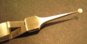 TEM grid balanced in tweezers
- Allow the nanowires to settle onto the grid undisturbed for 30'.
- Remove the droplet from the grid with your P200 set to 50 ul.
- Wash the grid by placing adding 15 uL of sterile H2O onto the grid. Immediately remove the water.
- Dry the grid by very gently touching the edge of the grid to a piece of blotting paper in a petri dish. Place the grid (shiny side up) onto the paper to transport to the TEM facility.
- To get there you should turn right as you leave our teaching lab and walk to the end of the hall to the "EXIT." Take the stairs down to the first floor and on your right you'll see a door to the core TEM facility that is run by the Center for Materials Science and Engineering. A member of the teaching faculty will be in the facility to examine your samples with you.

Part 2: TEM
DONE!
For next time
- Fig w image
- research proposal paragraph