Difference between revisions of "Understanding the lock-in amplifier"
Steven Nagle (Talk | contribs) (→Lock-in signal detection) |
Steven Nagle (Talk | contribs) (→Lock-in signal detection) |
||
| Line 25: | Line 25: | ||
|} | |} | ||
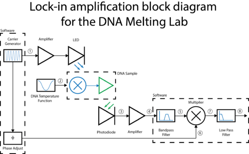
| − | A block diagram of the lock-in scheme is shown below. Implementing lock-in detection requires the ability to modulate the LED output with a carrier frequency and signal processing (in software) to recover the | + | A block diagram of the lock-in scheme is shown below. Implementing lock-in detection requires the ability to modulate the LED output with a carrier frequency and requires signal processing (in software in our case) to recover the non-modulated signal. In your case the non-modulated signal is the fraction of dsDNA versus time. To support these functions, the LED circuit must be modified to include a feedback brightness controller. In addition, the photodiode amplifier must be modified to accommodate the change in signal frequency range. In the control software, you will need to choose the LED modulation frequency as well as all filter frequencies to support your design. |
[[Image:DNA_Lock-in_Block_Diagram_20130725.png|500 px|center|Block diagram of lock-in amplifier for DNA melting]] | [[Image:DNA_Lock-in_Block_Diagram_20130725.png|500 px|center|Block diagram of lock-in amplifier for DNA melting]] | ||
Revision as of 22:39, 15 April 2014
Lock-in signal detection
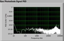
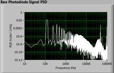
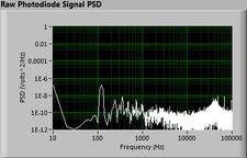
Lock-in signal detection provides some immunity to the very noisy lab environment. The plots below show typical Power Spectral Density measurements of noise in the 20.309 lab, a mix of optical and electronic noise. Fluorescent lighting creates a very strong technical noise at 120 Hz and harmonics. The lock-in technique moves the signal spectrum from the riotous low frequency realm to a calmer range of frequencies within the laboratory background noise spectrum. Noise in lab the may look different than in previous semesters (in which the default modulation frequency was chosen), so it may be useful to measure the noise spectrum before settling on a modulation frequency for your lock-in amplifier.
| |
||
| |
|
|
A block diagram of the lock-in scheme is shown below. Implementing lock-in detection requires the ability to modulate the LED output with a carrier frequency and requires signal processing (in software in our case) to recover the non-modulated signal. In your case the non-modulated signal is the fraction of dsDNA versus time. To support these functions, the LED circuit must be modified to include a feedback brightness controller. In addition, the photodiode amplifier must be modified to accommodate the change in signal frequency range. In the control software, you will need to choose the LED modulation frequency as well as all filter frequencies to support your design.
References


