Electronics Mini-Lab
Overview
During the next lab exercise on measuring DNA melting curves, you will build and debug several electronic circuits. This mini-lab will introduce you to the electronic components and test equipment you will use. A short answer-book style writeup is required. Items to include in your report are shown below in bold.
This mini-lab requires an understanding of basic circuits. If you need to review circuit concepts, start with the Electronics Primer page. If you have a lot of experience with electronics, ask one of the instructors about doing a stimulating mini-project instead of the mini-lab assignment.
Voltage divider
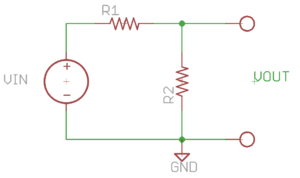
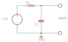
In the first part of the mini-lab, you will analyze and build a voltage divider. The divider circuit comprises two resistors and a voltage source, as shown in the schematic diagram. You will select the values for R1 and R2.
Before you build
Choose any two resistor values you like, but there are a few practical constraints. The resistors in the lab range in value from 1 Ω to 10 MΩ. Within that range, manufacturers only produce certain standard values. Check the supply bins or this table to see which values are available.
Power dissipation in resistors increases in proportion to the resistance and as the square of current, P = I 2R. The maximum power rating of the resistors in the lab is 1/4 Watt. Components operated at too high a power level may get very hot and fail. A noxious puff of smoke frequently accompanies failure. Even if a component operated at an excessive power level does not completely fail, it may no longer behave as specified. Ensure that the power dissipated by R1 and R2 does not exceed the maximum rating.
You will use an oscilloscope and a volt meter to measure voltages in the circuit. The oscilloscope has an input impedance of 1 MΩ. Connecting the oscilloscope probe to a node of the circuit is equivalent to placing a 1 MΩ resistor between that node and ground. In circuits that use very large resistors, the current flowing into the oscilloscope can significantly distort measurements.
Before building the divider circuit:
- Record the resistor values that you selected in a table, based on the color codes.
- Derive the gain of the circuit Vout / Vin, showing your work and the final expression.
- Plot or draw an IV curve consisting of calculated current I through R1 and R2 on the vertical axis versus and Vin on the horizontal axis, over the range 0 V < Vin < 15 V. Label your axes.
- On a separate set of axes, plot or draw the power dissipated in each of R1 and R2 as a function of Vin. Label your axes. Can your chosen resistors dissipate the highest power on the plot? If not, choose different resistors.
Measure the resistors with a digital multimeter
Go ahead and get the resistors for your circuit from the bins in the lab.
Verify the value of the resistors by reading the coded bands. Through negligence or malice of last semester's scholars, components occasionally end up in the wrong bin. Instructions for reading resistor markings are available at this website.
The resistance value encoded in the colored bands of the resistor is called the nominal value. A dictionary defines nominal this way: "stated or expressed but not necessarily corresponding exactly to the real value." In other words, the resistors you pick from the bin will have values that differ somewhat from their nominal value. The manufacturer of the resistors guarantees that the actual value will differ from the nominal value by no more than 5%. You can find the actual value by measuring the resistor with a digital multimeter (DMM). Use the actual value instead of the nominal value in your calculations to get more accurate results.
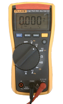
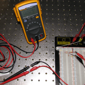
DMMs are multifunction instruments that usually include functions for measuring voltage, current, and resistance. They connect to component terminals through a pair of test leads. DMMs measure resistance by applying a small voltage across the test leads and measuring the resulting current flow. To get an accurate measurement of a resistor, its leads must be isolated from other circuit elements. If the resistor leads are connected to other components, current flowing through other paths will distort the measurement.
- Plug two test leads into the DMM.
- The black lead goes into the terminal labeled COM.
- The red lead plugs into different terminals depending on the measurement you are making. For resistance measurements, use the V/Ω terminal. The A terminal is for current measurements.
- Select the resistance mode, which is labeled with an Ω symbol.
- Connect the leads only to the resistor that you want to measure.
- Measure your resistors and record the the actual values in the table alongside the manufacturer-specified value from above. In an additional column, calculate the percentage difference between the two. Do the resistors fall within the manufacturer's specified tolerance of 5%?
Build the circuit
The next step is to build the divider circuit. Gather the components you will need:
- solderless electronic breadboard
- lengths of different colored wire to make jump wires
- wire strippers (located in the lab station tool drawers)
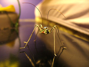
Most electronic components look like bugs. They have a central body with a bunch of gangly legs sticking out, called leads. The leads carry current from the outside of a component to its innards. One of the first challenges facing an aspiring circuit maker is to properly connect all the bugs' legs whilst keeping the circuit robust and orderly. Solderless electronic breadboards are a convenient platform for building circuits that might require a lot of debugging or frequent reconfiguration. Breadboards are flexible and easy to use, but they have a few downsides. They have high interconnect capacitance and resistance. If you don't know why that's bad, pay closer attention in lecture.
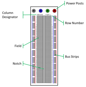
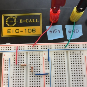
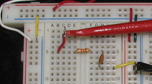
Breadboards have a large number of square holes in them called tie points. A single wire or component lead fits into each tie point. Spring-loaded contacts inside each tie point hold leads in place and provide an electrical connection. The images below show examples of solderless electronic breadboards. Sets of tie points are electrically connected in a pattern that allows component leads to be connected in almost any arrangement. The two central grids of tie points separated by a notch are called the field. Each row of tie points in the field is called a terminal strip. The terminal strips are numbered. Columns are designated by a letter. Within a terminal strip, the five tie points A-E are connected, and tie points F-J are connected. Points A-E are not connected to points F-J. Connections between component leads are made by running jump wires between tie points that are connected to each lead, as shown in the image above on the right.
The long lines of tie points to the left, right, and above the field are called bus strips. Bus strips are highlighted by red and blue lines. All of the tie points in a bus strip are connected together. Because most circuits have a lot of power and ground connections, the bus strips are almost always connected to the power supply. Using the bus strips as a power distribution network makes it easy to connect any terminal strip to power or ground with a short jump wire.
If you are unsure whether two holes on the breadboard are connected, insert short wires in the holes. Use the resistance or continuity features of the DMM to check if they are connected.
Assemble the divider circuit on a breadboard:
- Use the cutting jaws of the wire stripper to trim the resistor leads so that the component bodies will be close to the board.
- In addition to being untidy, leads that are too long may make unintentional contact with the metal under the breadboard.
- Mount the resistors by pressing component leads into the tie points in the field.
- Run jump wires to connect the divider to power and ground bus strips.
- Keep your wiring neat, close to the board, and easy to follow. A good way to do this is to route wires horizontally or vertically, making right-angle bends to change directions.
- Use the right length of wire. The right length of wire is the shortest length of wire that satisfies the previous guideline.
- Use the bus strips to distribute power supplies and ground.
Connect the power supply
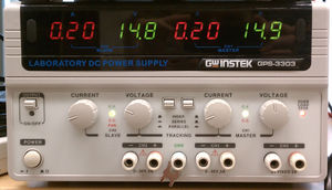
You will use a laboratory power supply to provide the voltage that drives your circuit. Each lab supply has three separate DC voltage outputs. One output always produces 5 volts with a current limit of 3 amps. The voltage and current limit of other two outputs is adjustable from 0-20V and 0-3A.
Pushbuttons on the lab supply allow you configure the two adjustable supplies 3 different ways: independent, series, or parallel. In independent mode, there is no connection between the two adjustable supplies. The voltage and current settings operate independently. In series mode, the plus terminal of one supply is connected to the minus terminal of the other. The series configuration is frequently used for circuits that require both positive and negative supplies. In parallel mode, the plus and minus terminals of the adjustable supplies are connected together. The voltage of both supplies is the same. The parallel configuration increases the maximum possible current to 6 amps.
The green ground terminal is connected to earth ground.
The supplies include an output enable function. When you turn the supply on, all of the outputs will be disabled. Press the OUTPUT button to enable all three supplies. A green LED indicates that the supplies are enabled. Press the OUTPUT button again to disable all three supply voltages.
The breadboard has four colored post terminals at the top right to facilitate power supply connections. These are called banana terminals. Each post terminal accepts a banana connector inserted at the top and a bare wire at the base. The banana terminals are not connected to any of the tie points, so it is necessary to run wires from the post terminals to tie points on the bus strips. Wires connected to the post should pass through the hole through the base of the post. Be sure that only bare wire touches the terminal. Insulation under the screw terminal may cause an intermittent connection. Secure the wire by tightening the colored plastic nut.
Use a cable with banana connectors on both ends to connect the power supply to the posts. You can find banana cables hanging on the wall near the time travel poster. Convention is to use black cables and connectors and blue bus strips for ground. Red bus strips are almost always used for power supplies.
The exposed metal screws on the bottom of the banana connectors can short to the metal optical table. Cover them with electrical tape to prevent a calamity.
Measure VOUT with a DMM
The DMM has modes for measuring DC and AC signals. In DC mode, the meter reads the average value of the test signal. In AC mode, the meter reads the root-mean-square value of a time varying signal. In this lab you will use DC mode, which is labeled with a solid line above a dashed line.
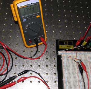
- Switch the DMM to DC voltage mode and connect the DMM test leads properly: Insert black in COM and red in VΩ.
- Make firm contact with the two leads across the terminals of R2.
- Record the voltage shown on the DMM for each input voltage Vin = 0, 2.5, 5, 10 and 15 V.
For voltage measurement, the DMM has an input impedance of 1 MΩ, so your measurement of output voltage should not be affected by the DMM. However, a lower input impedance can easily be simulated.
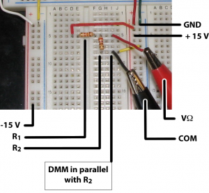
- Add a 1 kΩ resistor in parallel with R2 and record the new measured voltage on the DMM. Compare the measurement to a calculation of the expected result.
- Now remove the extra resistor and the DMM from the circuit.
Measure current with the DMM
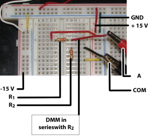
- Switch the DMM to DC current mode and connect the leads as shown in the figure above: Positive current is measured into the red lead, moved to the A socket of the DMM, and out of the black lead, remaining in the COM socket.
- Place the leads of the DMM in series with the circuit loop.
- Record the current through the circuit, if it is large enough, at each input voltage in units of mA.
- Plot these measured values on the same axes with the expected IV curve from above.
- At each voltage, calculate the resistance of R2 using Ohm's law and the measured current. Add these values to your table to compare to the DMM-measured and manufacturer resistance values.
For current measurement, the DMM has an input impedance of less than 1Ω, so your measurement of current should not be affected by the DMM. However, a higher input impedance can easily be simulated.
- Add a 100 Ω in series with the DMM and re-measure the current only at the highest input voltage. Compare the measured current value to a calculation of the expected value.
- Now remove the extra resistor and the DMM from the circuit.
RC low-pass filter
In this part of the lab, you will replace R2 with a capacitor to make a low-pass filter. You will measure the time constant and cutoff frequency of the filter.
In order to measure the filter response, it will be necessary to drive the circuit with a time-varying voltage. The lab power supplies produce a steady voltage output, which is not particularly useful for measuring frequency responses. It will be necessary to replace the power supply with a piece of equipment that generates an output that changes over time. You will replace the power supply with a function generator, which is a piece of equipment that can generate sine, triangle, and square waves. The amplitude and frequency of the function generator's output are adjustable. You will use an oscilloscope to measure the output of the filter.
Capacitors are available in the lab with a range of values from 0.1 - 10 nF. Check the supply bins to see what is available and choose a value for C1.
- Calculate the expected cutoff frequency of your filter
- If the frequency is below 100 Hz or above 10 kHz, you might want to rethink your capacitor or resistor choice. Change either the resistor or capacitor to get a cutoff frequency in this range.
- Replace R2 with a capacitor of the selected value.
Replace the power supply with a function generator
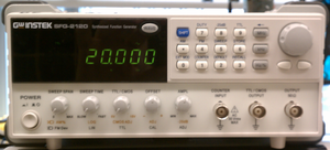
There are several types of function generators in the lab. The digital function generators allow you to enter frequencies on a keypad. Press one of the unit keys (Hz, kHz or MHz) to complete your entry. Use the decade selector knob and frequency dial to set the frequency of the analog function generators. The output frequency is adjustable between about 0.01 Hz and 10 MHz. Amplitude ranges from 0.1 V to 10.0 V.
- Disable the power supply and disconnect it from the circuit.
- Connect a function generator in place of the power supply.
- Attach a BNC cable to the Output connector on the front right of the function generator.
- Use a BNC to banana clip adapter and connect the function generator to the post terminals, or use a BNC to grabby clip adapter. There are also BNC to bare wire adapters in the lab.
- The center conductor of the BNC cable is the positive signal lead; the outer conductor/shield is the ground signal lead.
- Turn on the function generator.
- Set the frequency to about one tenth of your calculated cutoff frequency.
- Select a square wave output. (Press the WAVE button on the digital function generators or use the waveform knob on the analog generators.)
Connect an oscilloscope
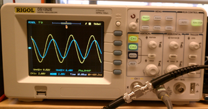
Oscilloscopes provide a graphic display of time-varying voltage signals. In the most frequently used mode, the oscilloscope screen shows a plot of voltage on the vertical axis versus time on the horizontal axis. The oscilloscopes in the lab have two inputs. Either or both of the inputs may be plotted. Two knobs adjust the voltage and time scales so that it is possible to display a wide range of waveforms. The display also includes status indicators and configurable waveform measurements such as amplitude, frequency, and phase.
The oscilloscope begins recording and displaying the waveform when it is triggered. There are several options to configure when the trigger occurs. One of the simplest modes causes a trigger when the input signal crosses a certain voltage level. The level for the trigger is can be adjusted with the "Level" knob.
Click these links for full documentation for the Rigol DS1052e and ATTEN ADS1022c oscilloscopes.
- Get two oscilloscope probes from the cable rakes on the wall next to the time machine poster.
- Connect the oscilloscope to the circuit.
- Connect the BNC connector on one probe to the CH1 oscilloscope input. Connect the probe to Vout using a small jump wire held in the retractable clip at the end.
- Connect the black alligator clip to ground.
- Connect the other probe to the CH2 input and to Vin.
- Set the oscilloscope vertical scale for each channel to 5 V per division.
- The Rigol oscilloscopes have one knob that controls the vertical scale for both channels. Press one of the channel select buttons before you adjust the knob.
- The ATTEN oscilloscopes have a knob for each channel. Software menu functions still require you to press the button for the desired channel.
- Set the scope to trigger on CH2.
Measure the low-pass RC filter
- Adjust the signal generator amplitude and oscilloscope horizontal scale until about you can see about three periods of the square wave.
- Measure peak-to-peak values of Vin and Vout.
- Measure the time required for Vout to increase by 63% of the difference between the minimum and maximum levels. This is the time constant of the circuit.
- Switch the function generator to sine wave mode.
- Record the amplitude of Vout at several frequencies over the range of 0.01 to 100 times the cutoff frequency.
- Plot the transfer function of your circuit.
Identifying unknown filter circuits
RC filters come in many flavors and each can be identified with the tools introduced thus far. All flavors can be analyzed as some combination of the low-pass filter explored and the high-pass filter. For example, a band pass filter is simply a combination of the the low- and high-pass filters, as is its sibling the band-stop filter. Both of these act as their name implies: Over a band of frequencies the signal is either passed or blocked, respectively.
To quickly analyze these filters in the lab, modify the technique of the last section. First, drive the circuit with a sine wave rather than a square wave. Second, convert the relaxation time into a characteristic frequency fc = 1/2πR1C1, referred to as the cut-off frequency (Take note of the 2π.). For the low-pass filter, if the input signal frequency is low compared to the cut-off frequency, the signal is not filtered and passes through. If on the other hand it is near, at, or above the cut-off frequency, then it will be partially or completely blocked, i.e., attenuated. Well above the cut-off frequency the attenuation increases linearly with signal frequency. The response of the high-pass filter is simply a mirror image with respect to the cut-off frequency. And responses of band-pass and band-stop filters are simply the superposition of a low-pass and a high-pass filter.
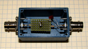
There are several metal boxes with unknown filter circuits inside, labelled "A" through "D". Your goal is to determine their transfer functions.
- Connect the function generator and oscilloscope to one of the black boxes (which are actually blue) using BNC cables.
- Set the scope to trigger from the input channel.
- Measure Vpp of both the input and output signals from 10 Hz to 10 MHz with at least one measurement per decade.
- Each box is a different filter type. Take enough data to confirm this.
- Plot the ratio of output to input Vpp versus frequency (as a log-log plot) for each black box.
- Repeat the previous two steps for each box, A through D.
- Draw circuits to model the observed behavior of each box. Note that one box is only subtly different than a similar box.
- In Matlab, use the
nlinfitfunction to fit the transfer function of the model to the observed transfer function. - What happens to the energy of the attenuated frequencies?
- Match the box below (left) with one of your data sets.
Photodiode I-V curve
In this part of the lab, you will examine how light falling on a photodiode affects its I-V characteristic. You will use a function generator and an instrumentation amplifier to make simultaneous measurements of voltage across and current through the photodiode and plot an I-V curve on an oscilloscope.
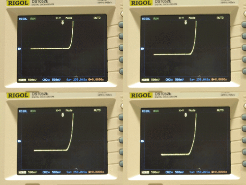
In the preceding sections of this lab, you used an oscilloscope to plot voltage signals versus time. The oscilloscope also has an X-Y mode. In X-Y mode, the oscilloscope plots channel 1 on the horizontal axis versus channel 2 on the vertical axis. Using X-Y mode, it is possible to use an oscilloscope to plot an I-V curve.
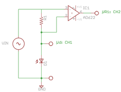
I-V curves usually show current on the vertical axis and voltage on the horizontal axis. Using the oscilloscope to plot VD1 on the horizontal axis is easy. Just hook the channel 1 probe across the photodiode.
It is not as straightforward to plot Idiode. The oscilloscope measures voltage, so first it is necessary to convert ID1 to a voltage. This can be done by placing a resistor (R1) in series with the photodiode. The voltage across R1 is proportional to the current through the photodiode.
It's a little harder than you might anticipate to measure the voltage across R1 with an oscilloscope. You might be tempted to hook the channel 2 probe across R1. Unfortunately, the ground leads of the oscilloscope probes are wired together. Connecting the probe in this way causes a short from R1 to ground. Because the ground leads of the probes are wired together, it is a very good idea to hook probe ground clips only to the ground node of your circuit.
An instrumentation is a type of amplifier that produces an output equal to the difference between the voltages at its two input terminals. The instrumentation amplifier shown in the schematic diagram computes VR1 = Vin - VD1. The input terminals of the instrumentation amplifier have very high input impedance, so current flowing into the instrumentation amplifier inputs is negligible. There are many kinds of instrumentation amplifiers available. In this lab, you will use an integrated circuit (IC) instrumentation amplifier, part number AD622 manufactured by Analog Devices. [Click here] for the AD622 data sheet.
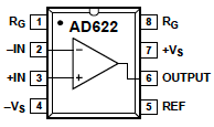
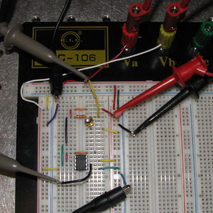
The instrumentation amplifier comes in an 8 pin plastic package called a dual-inline package (DIP). The leads on the package have the same spacing as the tie points on the breadboard, so the amplifier can be inserted directly into a breadboard. The arrangement of component leads for the instrumentation amplifier is shown at right.
Construct the photodiode circuit
- Make sure your power supply is disabled.
- Mount the instrumentation amplifier so that it straddles the notch.
- Connect the signals as shown in the schematic to pins 2 and 3. The output is pin 6.
- Use a 10KΩ resistor for R1.
- Connect the REF signal on the amplifier (pin 5) to ground.
- Configure the power supply for series mode.
- Set the power supply for +/- 15V.
- In series mode, the negative terminal of the left supply will be at -15V. The positive terminal of the left supply and the negative terminal of the right supply will be connected together inside the power supply. This is the ground potential. The plus terminal of the right supply will be at +15V.
- Connect the power supply leads to the +VS and -VS pins: pins 7 and 4, respectively.
Procedure
- Connect the function generator to provide Vin to the circuit. Configure the function generator to apply a triangle wave between ± 1-3 V at 1 kHz.
- Connect Channel 1 of the oscilloscope to Vd
- Connect Channel 2 of the oscilloscope to VR1 (the output of the instrumentation amplifier).
- Set the oscilloscope to X-Y display mode.
- With the photodiode covered, save the curve to a USB memory stick.
- Load the curve into Matlab and plot the I-V curve
- Remember to convert the resistor voltage to current.
- Repeat the measurement for several intensities of light illuminating the diode.
- Plot the curves for all light intensities on the same set of axes.
- What operating condition of the photodiode is best for measuring light intensity?

