DNA Melting Part 1: Measuring Temperature and Fluorescence
Revised to the more focused functional groups in the block diagram. Shortened text to remove repeats within, extraneous info and some info that is covered in the Introduction and Outline page. Targeted at 3 paragraphs. Limited to Part 1 only. Removed picture of old setup. Block diagram may be sufficient instead of both.
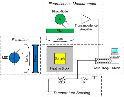
You will construct a basic DNA melting instrument consisting of the five functional groups shown in the block diagram:
- excitation
- heating
- fluorescent detection
- temperature measurement
- data acquisition and control
A metal block will hold a sample vial in the excitation light path and transfer heat to the sample. The sample contains a combination of DNA, SYBR Green I and a salt. Recall that SYBR Green I fluoresces when it is bound to double stranded DNA (dsDNA) by a factor of up to 1000x compared to when it is bound to single stranded DNA (ssDNA). Detection of this fluorescence provides a relative measure of the fraction of dsDNA to total DNA, which can be compared to predictions from a thermodynamic model.
The dye has a peak sensitivity to blue light at 497 nm so a blue LED will be used to illuminate the sample. The dye emits green light with an emission peak at 520 nm. A photodiode will be placed at 90° to the LED source to detect the green light emitted by SYBR Green I. Because LEDs have a fairly broad spectrum, first a moderately narrow band-pass filter will be used to limit the excitation wavelength to between 450 and 490 nm. Then a complimentary long-pass emission filter will be placed between the sample and detector to pass only wavelengths longer than 515 nm. This filter combination, when used with this dye system, eliminates any background signal due to the excitation light.
The sample block will be heated by a TEC and its temperature measured by an embedded thermistor. Also, since photodiodes produce a very small amount of current, a high gain amplifier will convert the photodiode current into a measurable voltage. The DAQ and PC will digitize the amplified photodiode and thermistor signals. A Matlab program is provided to record these fluorescence and temperature signals over time and save the data to a file. The file can then be loaded into Matlab for analysis, or if you prefer, Python or equivalent where the signals will be converted into dsDNA concentration and sample temperature. Finally, the dsDNA sample melting temperature will be estimated from a plot of df/dT vs T and from a comparison to the thermodynamic model.
Mechanical subsystem
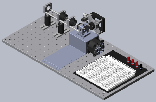
Mechanical support for the heating block, sample and optics will be built on a portable optical breadboard from ThorLabs. Most of the components in the lab are from this supplier because the selection is large, the quality is quite good and the price reasonable. Although you are free to modify the design as the lab progresses, begin a build from the standard design shown above and demonstrated by the example in the lab. Gather the following Thorlabs components but do not start to assemble.
- 1 MB1224 optical breadboard
- 2 TR2 posts
- 2 PH2 post holders
- 4 CP02 cage plates
- 2 SML05 lens tubes
- 2 CL5 clamps (or similar)
Also gather these components:
- 1 Aluminum heating block
- 1 sheet metal support bracket
- various screws/washers and other hardware
Thermal subsystem
Refer to the figure below as well as the reference setup in the lab and be sure to understand each aspect as you build your own. Most components have a well-defined position and purpose in this part of the lab.
Optical subsystem
Build an optical system to illuminate the sample and capture the emitted fluorescence light. See the figure for the name and location of each component. There are a variety of ways to construct the apparatus. A good design will be compact, stable, and simple.
Electronics subsystem
Data acquisition hardware subsystem
Instrument control and data acquisition software subsystem
Part 1 experimental procedure
.
.
.
Building the optical system
As mentioned above, the optical system consists of an LED, an excitation filter, a sample cuvette, a heating block (because it contains mechanical apertures), an emission filter, optional lenses, a photodiode, and associated mounting hardware. Each of these components present design constraints in addition to their intended purpose. You should discuss these in your lab report. Construct your system on an optical breadboard. The breadboard has a grid of tapped holes for mounting all kinds of optical and mechanical hardware. ThorLabs manufactures most of the hardware stocked in the lab. A few of the components that you will certainly use include: TR2 1/2" diameter posts and PH2 post holders, CP02 cage plates, and SML03 and SML05, 1" diameter lens tubes. You may reference the TA setup to get started.
There are a variety of ways to construct the apparatus. A good design will be compact, stable, and simple.
Excitation light collimation
You will use a high-brightness blue LED manufactured by LedEngin, Inc.[1] to excite the sample. Light from the LED diverges in a cone with an angle of about 100°. It will be advantageous to include lenses in your system to collimate light from the LED onto the full area of your sample. In your report, talk about why you would not focus the light on the sample.
This LED has a dominant wavelength of 465 nm. A Chroma Technology D470/40 bandpass filter[2] eliminates unwanted parts of the spectrum that might interfere with detection of the fluorescence signal, such as the very wavelengths you want to measure in the fluorescent emission. The filters have exposed, delicate coatings and must be handled carefully[3]. In addition, the filter works better in one direction than the other[3].
Emitted fluorescent light collection
The Thorlabs SM05PD1A[4] photodiode is mounted in a short tube with SM05 threads. Use an SM1A6[5]adapter to mount the photodiode in a CP02 cage plate or lens tube. Mount the photodiode assembly to the breadboard at 90° to the LED. Also hold the Chroma E515LPV2 emission filter[6] in front of the photodiode. If you wish, use one or more lenses to focus light from the sample onto the detector. In your lab report, discuss the primary design goals for these optics in terms of concepts you learned in the Microscopy module.
Do not connect the sample block to any other pieces of metal — this will draw off heat and affect your instrument's performance. Do not connect the sample block to the fluorescence detection arm. This will cause your heating block to make poor contact with the TECs. Make sure your optical path is mechanically stable during and between your experimental runs.
Building the Electrical System
LED driver
The LED will be powered using 5 V by placing the LED in series with a ~25 Ω resistor. Use the fixed 5 V output from your Instek power supply.
| |
Don't forget the resistor. Directly connecting the 5 V will blow out the LED without a low current limit at your supply. |
Heating control
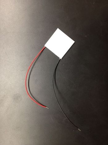
After ensuring that the power is off, directly connect a Diablotech power supply to a double TEC stack using the male 4-place connector on the supply with two yellow and two black wires that supplies 12 V and up to 15 A, to the connector provided on the counter top near the optical samples. The connector provided is a female 4-place Molex connector with a black and white twisted pair of wires coming out. It is best to connect the TECs to this connector using blue or gray "wire nuts" that are available in the DNA Melting Lab drawer under the hot plate. Keep the white/black wire and connector with your setup. Each station will have an identical Diablotech power supply.
If you connect the white wire of the connector to the red wire of the TEC then the top side of the TEC, as pictured below, will be the hot side. Ask a TA or Instructor for assistance if needed.
Be sure that you have attached a heat sink to the under side of your aluminum bracket, the TECs should rest on this, with a very thin film of thermal grease between them. Also, it is easier if you attach the fan to your bracket before assembling the heat sink and TECs.
When you are ready to heat your sample later on, you will simply switch on the Diablotech. When you the block reaches no more than 100 C, switch it off and your sample will passively cool down.
Temperature detection
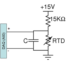
The electrical resistance of most materials varies with temperature. An RTD is a special resistor (usually made out of platinum) that exhibits a nearly linear change in its value with temperature. An RTD may be used to accurately measure temperature by including it as an element in a voltage divider. As the resistance of the RTD changes, so will the voltage across it.
A PPG102B1 RTD from US Sensors[7] has been pre-mounted on the DNA heating block. This RTD has a nominal resistance of 1 kΩ and its value increases with temperature. Note that the maximum current carrying capacity of this device is 1 mA, so if you alter the voltage divider design, be sure that no more than 1 mA flows through the RTD. To test basic functionality of your circuit, you can press your finger on the RTD while your lab partner measures the divider voltage with a digital multimeter. Or you can see the temporal effect by doing the same measurement with your oscilloscope.
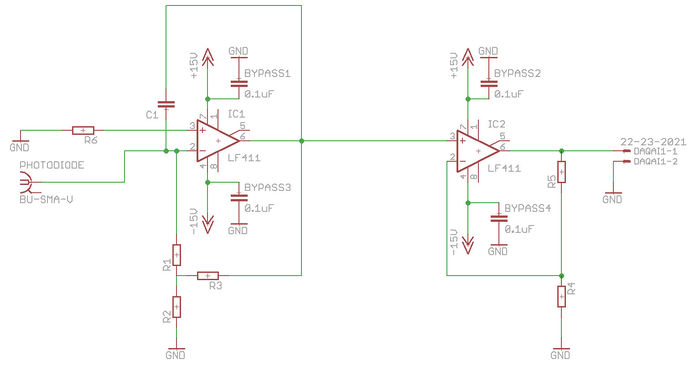
The diagram to the right shows the suggested temperature detection circuit. The capacitor across the RTD implements a low pass filter whose purpose is to eliminate noise in your temperature reading. Consider the following points when choosing a capacitor value: What noise sources are you attempting to filter. What is the cutoff frequency above which you want to attenuate said noise? Think also about the time constant of the temperature change you wish to observe, you don't want to filter your desired signal. Compare this to the time constant of your filter? If it is too large compared to the rate of change of temperature, it could cause a delay in your temperature reading.
Photodiode signal amplification
Excited SYBR Green I molecules emit photons in all directions, some of which pass through the aperture in the heating block then the emission filter and then strike the photodiode. This generates a tiny current in the photodiode, which must be converted to a voltage and amplified to a level that can be conveniently measured. From past experience, the photodiode output current could be on the order of 15 nA but this depends on excitation light flux and your emission collection optical system design. Can you calculate it from first principles, starting with the current applied to the LED?
The amplification circuit
The NI-DAQ interface card used in lab can digitize a voltage between positive and negative 10 V. A first approach to providing this voltage swing at the digitizer inputs was demonstrated in the homework: a transimpedance amplifier with a gain of approximately 7x$ 10^8 $ V/A would produce this voltage amplitude if the photodiode current is as stated above. In your report, describe why we could not simply use a resistor, and omit the op-amp. You should also realize from the real electronics lecture, and comment in your lab report, that implementing the photodiode amplifier in a single stage presents its own set of challenges. Because of this it is suggested that you implement a two-stage amplifier as shown in the figure below. Your job as circuit designers will be to fill in the appropriate feedback resistor and capacitor values in order to achieve the desired gain at the output while also filtering unwanted noise sources where possible. If you have another topology in mind, feel free to discuss with your TA and/or Instructors. We like variety and new ideas.
Think carefully about how you want to distribute the gain of the system across the stages: how does feedback affect the noise of the amplifier? What are the dominant sources of noise in the DNA melting setup? Which ones do you have most control over. How could you reduce them instead of trying to filter them? By applying your new knowledge of feedback and transfer functions, you should be able to determine the optimal gain configuration of each stage for lowest output noise.
Practical matters
As with most amplifiers, care should be taken with lead dress, component placement and supply decoupling in order to ensure stability.
In theory, there is no difference between theory and practice. But, in practice, there is.
The universe is rife with electrical noise. Keeping the noise out of sensitive electronic instruments requires a great deal of care. Unfortunately, electronic breadboards are a poor environment in which to construct high gain amplifiers. A few simple tricks can improve things.
- Use power supply bypass capacitors. Connect a large capacitor between all supply voltages and ground, close to the point of use. Large, electrolytic capacitors of at least 0.1 μF work well for this purpose. Electrolytic capacitors are polarized. Make sure to put them in the right direction (If put in wrong, they may explode, and they will definitely start to smell bad.).
- Use the binding posts on the breadboard to connect your power supplies and be sure to strip enough insulation for good contact.
- Use the black post for ground, and, via several wires, connect it to the upper, horizontal blue "minus rail" on your breadboard. Then connect this to each of the vertical blue "minus rails." Use these for all local ground connections. In your lab report, comment on why you might want to connect several wires between the black post and the top, ground rail. If you need help with this practical matter, talk to an Instructor or TA.
- Power Supplies: Use a separate power supply for the op-amp circuits (+/-15 V supplies), LED driving circuit (5 V supply), and the heating control (12 V supply).
Even with these optimizations, it will be important to keep your wiring short and neat. A neat circuit works better, because it will be easier to debug and visualize. At the high gain of this circuit, local field coupling, between the circuit and your fingers, for example, can cause disturbances in your amplifier output. For this and related reasons, the amplifier and its wiring will be susceptible to physical movement, so prevent things from getting bumped during experimental runs. Low, short wire runs will help alleviate all of these issues.
A note about resistors and capacitors: recall that resistors introduce thermal noise, while capacitors do not. Therefore, the optimized system will use as low resistor values as are reasonable in filters and feedback paths.
Testing the circuit
The circuit is designed to amplify a small current input into a easily measured voltage. To test the circuit, a suitable current source can be used in place of the photodiode. Since the input to the circuit (at IC1 pin 2) is at virtual ground (= 0V), a voltage source in series with a large value resistor will produce a small current proportional to the test voltage. The largest resistor value available in the lab is 9.1MΩ. For finer control of the current, this resistor may be combined with a resistor divider to attenuate the input current. For example, for the circuit shown would give a current of 10nA per volt.
Use a digital signal generator as Vtest and oscilloscope to measure Vtest and the output of the circuit both at IC1 pin 6 and IC2 pin 6. Verify the gain and low-pass cutoff frequency of the circuit. It’s very easy to make an order of magnitude error when selecting components, so it’s important to test the frequency response. If the circuit does not act as expected, here are some items to check:
- Verify that all your component connections are correct and match the design. Check that wires and components are properly seated in the breadboard and not suspiciously loose. Use the ohm-meter function of the digital multi-meter to verify continuity.
- Verify that power is actually getting to the op-amps, i.e., +15V on pin 7 and -15V on pin 4.
- Verify that pins 2 and 3 (the V- and V+ inputs to the op-amp) are equal.
- For 0 nA input, you may still see a significant offset voltage at IC1 pin 6 (50-100mV, this is due to an inherent input offset voltage in the op-amp itself), which may cause IC2 to saturate (output voltage > 10V). You may be able to reduce this voltage by lowering the ratio of R3 to R2 while increasing R1 to preserve the gain.
When the circuit is working as expected, connect the photodiode. Use any convenient light source to excite the photodiode and verify that the circuit output changes in response. Use the emission filter and/or neutral density filter to cut down on the light intensity.
Once your apparatus is built, use samples of fluorescein (~ 30uM concentration) as a stand-in for SYBR+DNA (fluorescein is cheap, non-toxic, and will not bleach as quickly as SYBR) to test and tune the optics.
PC Data Acquisition System
The DAQ
Each lab PC is equipped with a National Instruments USB-6212 or USB-6341 data acquisition (DAQ) card.
The USB-6212[8] has 16, 16-bit analog input channels which can, in sum total, accomplish 400 thousand samples per second (400kS/s). That is, if there are two channels, each one will be alternately sampled, and EACH sampled at 200kS/s. A multiplexer sequentially selects from among the 16 single-ended and 8 differential input signals. The card also supports two 16 bit analog output channels with an update rate of 250 kS/s and an output range of +/-10 V and up to +/-2 mA.
The USB-6212 also has 32 digital input/output channels and a digital ground. A 50 kΩ pull-down resistor is typically used in series with connections to these channels.
The USB-6341[9] is s little more powerful. It has 16, 16-bit analog input channels which can, in sum total, accomplish 500 thousand samples per second (500kS/s). Again, a multiplexer sequentially selects from among the 16 single-ended and 8 differential input signals. The card also supports two 16 bit analog output channels but they have an update rate of 900 kS/s and an output range of +/-10 V and up to +/-2 mA.
Finally, the USB-6341 has 24 digital input/output channels and a digital ground, as well as 4, 100 MHz counter/timers.
Summary of DAQ inputs/outputs
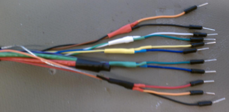
A special connector has been prepared for you, connected as shown below. The connections and cable wire colors are also summarized in a memo.
| Signal Name | Signal Location | Ground Location | Pin wire color |
|---|---|---|---|
| DAQ Inputs | |||
| RTD | AI0+ | AI0- | +Orange / -Black [lone pair, not with third (red) wire] |
| Photodiode | AI1+ | AI1- | +Green / -White |
Things to watch out for
- The DAQ has only one ADC (analog-to-digital converter), which is multiplexed between all of its analog inputs. The ADC has input limits of +/-10V. If one input is outside this range, it will get confused and give nonsensical values for all inputs. The upshot is, if either your temperature or fluorescence measurement is nonsensical, check to make sure the others are not receiving a higher voltage, like 15 V or 12 V, at the DAQ.
- If you short-circuit your DAQ, it will also get confused. One symptom of this is the data acquisition program refusing to run, for example, wrongly complaining that the limits on the band-pass filter do not satisfy some condition. If this happens, unplug and re-plug the DAQ and use the Measurement and Automation software to check its condition and the test panels therein to check signals on the AI0 and AI1 inputs.
PC and Software
Lab station PC
Log in to your lab station PC using the credentials provided. The computer is connected to the lab station DAQ device via USB. Check this connection before you start the Matlab GUI.
Matlab GUI
The Matlab DNA Melting GUI is called DNAMelter.m and is located in the CourseMaterials/Labs/DNAMelting. You may make a copy in your directory of choice, double click that copy to open the code in Matlab, then run the code via the Run button.
Follow the instructions in the GUI. Graphs and readouts are labeled.
At the end of a run, use the "Save Data" button to save to a file. The data will be tab-delimited and can be read into Matlab with the load command.
Troubleshooting: If Matlab gives you a data acquisition error, for example, "NO DATA ACQUISITION DEVICE FOUND!", open the Measurement and Automation Explorer ("MAX"), open the Devices and Interfaces drop-down on the left side, and make sure there is only one "NI USB-6xxx" entry and that it is called "Dev1." If it is not, or there is more than one device listed, physically disconnect the USB cable from your DAQ, then delete all "NI USB-6xxx" entries, then reconnect your DAQ, then verify that one entry reappears and that it is called "Dev1." Try to run the DNAMelter program again, and/or close it, re-open it, and run it again. If this does not work, consult a TA or Instructor.
More info: DNA Melting: Using the Matlab DNAMelter GUI
Debugging the apparatus
- Use your finger to make sure the temperature circuit is working properly. Touching the washer over the RTD will produce a response if the circuit is working.
- Cover and uncover the photodiode, exposed to room light, to verify operation of the fluorescence measurement system. You can use one or more neutral density filters (NE20A) to reduce the room or LED light down to levels close to that of the fluorescence from your DNA.
- Close your emission optical path to shield your photodiode from ambient light. Can you measure the difference between a cuvette filed with water and one with DNA and SYBR Green?
- Observe every electrical signal node with the oscilloscope. Are any signals noisy? Is there a way to improve the quality of poor signals?
- Watch the fluorescence readout over time. Is it stable or does it drift even when block temperature is constant?
- Is your temperature reading nonsensical, for example, far too large or negative? Make sure you are using 15 V supply and 15 kΩ resistor. Also make sure that the DAQ input is placed across the RTD not the 15 kΩ resistor.
- Is your LED turning on?
Part 1 Experimental procedure
Once your instrument is running to your (and your TA's) satisfaction, you will measure three consecutive melting curves for a 20 bp DNA sample. If you have time, you can run additional experiments with other samples. For example, you could gather additional base pair number, ionic strength, or mismatch data points and evaluate your instrument's ability to discern the different melting points of these samples.
Experiment steps
- Open and run the
DNAMelter.min Matlab and follow the instructions there. - Confirm that you can accurately measure block temperature, then take your block through one temperature cycle
- Next prepare a sample as described below, use our stock of "junk" DNA, and place cuvette in heating block, but do not heat yet.
- First, at steady room temperature, use the DNAMelter GUI to record photodiode output and measure the signal to noise of your instrument with this sample. (See instructions below)
- Use the DNAMelter GUI to record RTD and photodiode output during heating and cooling, and save the data.
- Repeat the first few steps with a good sample, then measure more curves (with the same sample) only enough to feel confident of your data, and save the data for each run.
- Record melting curves for additional sample types if desired. Talk to your TA or Instructor, we have some old DNA of different types.
- Make any modifications to the code that will help you. Be sure to save your own copy in your own directory.
Making a sample
Sample prep steps
- Pipet 500 μl of DNA plus dye solution into a glass cuvette. (Ask your TA or an Instructor for one of these reusable, and expensive, cuvettes).
- Pipet up to 200 μl of mineral oil on top of the sample to help prevent evaporation. It will help to pipette into the corners first. Be careful not to get oil on the cuvette sides far above the sample. It will run down during your experiment and cause shifts in the photodiode signal. Put a disposable top (available in a drawer under the bench) on the cuvette.
- Keep the sample vertical to make sure the oil stays on top.
- You should be able to use the same sample for several heating/cooling cycles (What makes it go bad? What can you do to limit this effect?). Only discard it if you lose significant volume due to evaporation or your signal gets too low.
- If you need to leave the sample overnight, store it in the lab refrigerator.
- When not being used, you should protect the sample from light so that photobleaching is minimized.
To clean your glass cuvette between samples, flush with alcohol in the waste container, rinse with water at the drain, and if you wish by also soak/rinse with the Lysol cleaner. Whatever you do, your last rinse should be with DI water. You can suck out residual liquid with the vacuum and drawn pipette to the left of the sink.
Measuring DC signal to noise
Carry out a simple test of the signal to noise ratio (SNR) of your instrument by comparing your signal with a sample present to your signal with no sample present. This process includes a fresh sample of DNA in a cuvette, to be inserted into your heating block when it is steady at room temperature.
Start by using the DNAMelter GUI to record the photodiode signal with no sample present. Click "Clear Data" in the GUI and wait about 10 s.
Next insert your cuvette and record for another 30 s to 1 min or more. Be sure that all other conditions of your instrument are exactly the same when you have the sample present and when you do not.
Analyze this data in Matlab to calculate the SNR.
First separate the data into two parts, the part with no sample, and the part with a sample present. In Matlab or Python, fit a straight line to the data with no sample present, this is your background level. Calculate the rms value of this data, this is your zero signal noise.
Next fit an exponential (or another straight line) to the data with a sample present. The exponential comes from the fact that the SYBR Green is bleaching when exposed to the bright excitation illumination. You may see a pronounced effect if you measured the sample for more than a minute. Here the value is your signal plus background, and the rms value is your signal noise.
Compare the levels of these curves, this difference is your signal. Divide the signal level by the signal noise, take the base-10 log, and multiply by 20. This is your exceedingly simple SNR, signal to noise, in dB. (Is your background noise the same as your signal noise?)
You will carry out a much more robust measurement of SNR for your Phase II instrument, but this type of SNR calculation is a reasonable place to start.
Sample disposal
Lab manual sections
- Lab Manual:Measuring DNA Melting Curves
- DNA Melting: Simulating DNA Melting - Basics
- DNA Melting Part 1: Measuring Temperature and Fluorescence
- DNA Melting Report Requirements for Part 1
- DNA Melting Part 2: Lock-in Amplifier and Temperature Control
- DNA Melting Report Requirements for Part 2
References
- ↑ Datasheet for Blue LED from LEDengin
- ↑ D470/40 Bandpass filter spectrum
- ↑ 3.0 3.1 Handling, orientation, and care of a coated optical filter
- ↑ Thorlabs SM05PD1A photodiode
- ↑ Thorlabs SM1A6 adapter
- ↑ Chroma EV515LPv2 Long pass filter spectrum
- ↑ Datasheet for PPG102B1 RTD
- ↑ Datasheet for the USB-6212
- ↑ Datasheet for the USB-6341
Subset of datasheets
(Many more can be found online or on the course share)

