Difference between revisions of "DNA Melting Part 1: Measuring Temperature and Fluorescence"
Steven Nagle (Talk | contribs) (→Excitation light collimation) |
Steven Nagle (Talk | contribs) (→LED driver) |
||
| Line 77: | Line 77: | ||
The LED used in this lab can consume 1.5 Amps of current when driven to its full range, but this is more than 10x the light you will need. In fact, you will need only roughly 100 mA, but even this low current is 50x what the analog voltage output sources in the [[20.309:DAQ System|20.309 USB-6212]] DAQ systems are capable of driving. And even if there were enough current available, the steepness of a diode's I-V curve results in large swings in current for small changes in supply voltage. LED radiant flux is proportional to current, so a current source tends to provide a more stable light output. | The LED used in this lab can consume 1.5 Amps of current when driven to its full range, but this is more than 10x the light you will need. In fact, you will need only roughly 100 mA, but even this low current is 50x what the analog voltage output sources in the [[20.309:DAQ System|20.309 USB-6212]] DAQ systems are capable of driving. And even if there were enough current available, the steepness of a diode's I-V curve results in large swings in current for small changes in supply voltage. LED radiant flux is proportional to current, so a current source tends to provide a more stable light output. | ||
| − | To implement a current source to drive your LED, you will be using a [http://en.wikipedia.org/wiki/Darlington_transistor Darlington Transistor]. This is a special device in which one transistor drives another to provide higher input-output current gain. At the LED current levels for your instrument, the TIP120 will be providing a current gain of about 500. A [http://en.wikipedia.org/wiki/Transistor#Usage transistor] is a three terminal device in which the voltage or current at one terminal controls the voltage across, or current through, the other two terminals. In our case, the TIP120 acts like one BJT consisting of a Base, Emitter, and Collector, and should be wired into the circuit shown | + | To implement a current source to drive your LED, you will be using a [http://en.wikipedia.org/wiki/Darlington_transistor Darlington Transistor]. This is a special device in which one transistor drives another to provide higher input-output current gain. At the LED current levels for your instrument, the TIP120 will be providing a current gain of about 500. A [http://en.wikipedia.org/wiki/Transistor#Usage transistor] is a three terminal device in which the voltage or current at one terminal controls the voltage across, or current through, the other two terminals. In our case, the TIP120 acts like one BJT consisting of a Base, Emitter, and Collector, and should be wired into the circuit shown in the diagram. We will use the base contact of our TIP120 to accept a small amount of current from an op-amp, which will cause the TIP120 to conduct a much larger current between it's collector and emitter, in turn allowing nearly the same level of current to flow through the LED. |
| − | As described in lecture, the op-amp will be used to linearize the behavior of the TIP120. Here the LED and transistor are inside a feedback loop extending from the output of the op-amp, through the base-emitter conduction path in the TIP120, and back from | + | As described in lecture, the op-amp will be used to linearize the behavior of the TIP120. Here the LED and transistor are inside a feedback loop extending from the output of the op-amp, through the base-emitter conduction path in the TIP120, and back from the top of the 1 Ohm resistor, whose voltage drop is thus fed-back to the negative input node of the op-amp, completing the loop. Recall that this is simply a buffer implementation, with gain of 1, where the feedback voltage is directly proportional to the LED current. Notice that in this way the current through the LED is exactly equal to the voltage applied to the op-amp positive input by the DAQ. (Remember the golden rules.) |
| − | Note | + | Note: if the LED is too bright then the sample will become photobleached very quickly. In the Labview VI for Part 1, you are able to set the voltage supplied to the op-amp. |
| − | Note also that the voltage to the LED comes from the fixed 5V supply, modulated by the TIP120, whereas the op amp operates on +/– VCC (+/-15V in your setup). | + | Note also that the voltage to the LED comes from the fixed 5V supply on your lab station's INSTEK GPS-3303 power supply, modulated by the TIP120, whereas the op-amp operates on +/– VCC (+/-15V in your setup). |
{{Template:Safety Warning|message=Double check your wiring before connecting the LED. The LED can be damaged by excessive current. Remember the rule of thumb: if you can't keep your finger on a component indefinitely, it is too hot. Reduce the offset and amplitude of your driving current to protect the LED as well as minimize photobleaching.}} | {{Template:Safety Warning|message=Double check your wiring before connecting the LED. The LED can be damaged by excessive current. Remember the rule of thumb: if you can't keep your finger on a component indefinitely, it is too hot. Reduce the offset and amplitude of your driving current to protect the LED as well as minimize photobleaching.}} | ||
Revision as of 14:26, 29 August 2011
Overview of the apparatus
The DNA melting apparatus you will construct consists of five major subsystems:
- optical excitation,
- optical emission measurement,
- heating and cooling,
- temperature sensing, and
- electronic data acquisition.
Major components of these subsystems include, respectively, an LED, your DNA sample with SYBR Green I label, a photodiode and amplifiers, a thermoelectric heater/cooler (or TEC, also called a Peltier cooler/heater because it employs the Peltier effect>, a resistance temperature detector (RTD), and a PC data acquisition system (DAQ).
SYBR Green I is a fluorescent dye with peak sensitivity to blue light just below 500 nm, and the dye emits green light with an emission peak at about 520 nm.[1] You are encouraged to look at the spectrum here. Once you have your sample you will be able to easily observe this behavior –- a room-temperature sample of dsDNA and SYBR Green I looks yellow from the combination of blue excitation and green fluorescence. At higher temperatures, when there is no dsDNA to bind the dye, the sample will appear blue or clear. In order to produce a melting curve, your apparatus will measure the amount of fluorescent emission from the SYBR Green I dye over a range of temperatures.
Fluorescence intensity will be measured by the photodiode (and associated optical system to gather more light and concentrate it on the photodiode). Temperature will be measured by the RTD, which is a kind of resistor that predictably varies in value with temperature. The sample will be heated by the TEC. The DAQ and PC will record the signals from the photodiode and RTD. These signals must then be processed to convert them from raw voltage into temperature and fractional dsDNA concentration, f. The melting temperature, Tm, can be estimated from a plot of f vs. Tm of f vs. dTm/dt (Tm differentiated with respect to time).
Temperature will be measured by an RTD, which is a kind of resistor that predictably varies in value with temperature. Fluorescence intensity will be measured by a photodiode (and associated optical system). The sample will be heated by a thermoelectric device. A computer data acquisition system will record the signals from the photodiode and RTD. These signals must be processed to convert them from raw quantities to temperature and relative dsDNA concentration. The melting temperature, Tm can be estimated from a graph of this data or its derivative.
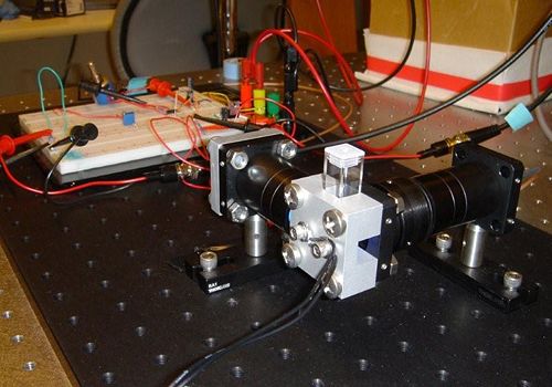
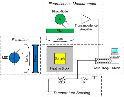
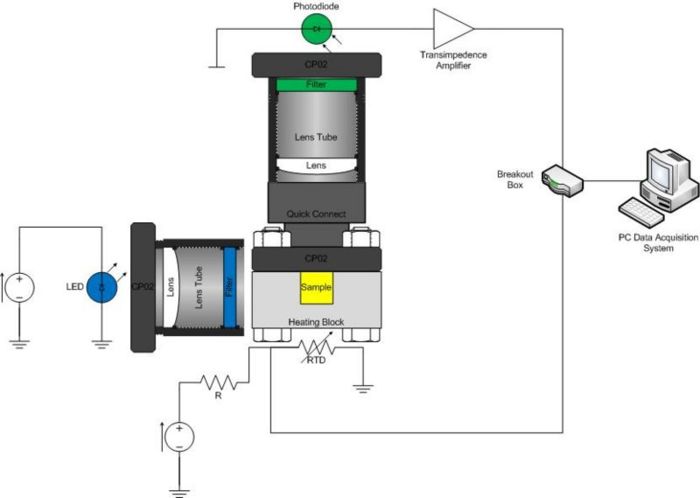
As shown in the diagram, an aluminum heating block holds a cuvette containing the sample under test. The sample contains a combination of DNA, SYBR Green I, and a salt (either KCl or NaCl, it doesn't matter which). In addition to being a convenient holder, the block transfers heat to the cuvette and it's sample, while also allowing the block's temperature to be measured without affecting the block temperature. (In your report, tell us about the practical problems with this approach and ways to improve it.)
Light from a blue LED illuminates one side of the cuvette. A 470 nm bandpass optical filter between the two shapes the output spectrum of the LED so that only the desired wavelengths of light fall on the sample.
A photodiode placed at 90 degrees to the LED source detects the green light emitted by SYBR Green I bound to the minor groove of dsDNA. The photodiode is placed after a 515 nm long pass optical filter to ensure that only green and longer wavelength light is detected. (In your report, describe how you ensure that only the fluorescent light given off by the sample falls on the photodiode.)
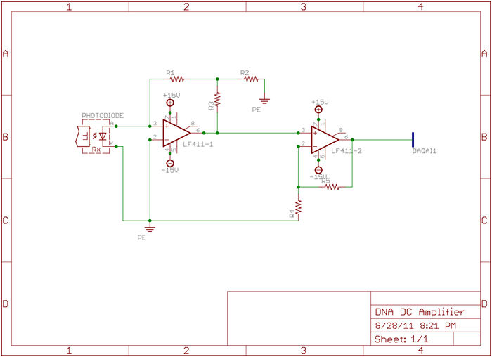
Since photodiodes produce only a very small amount of current, it will be necessary to build a very high gain amplifier to produce a signal that is measurable by the DAQ. Photodiode amplifiers can be challenging because many of the non-ideal characteristics of op amps become apparent at high gain. For this reason it is suggested that you build a two-stage amplifier. And furthermore it is suggested that your first stage be a transimpedence amplifier like the one shown in the figure. (In your report, comment on why a transimpedence amplifier is better for photodiode output amplification.)
An RTD attached to the heating block and wired to a voltage divider provides an indication of temperature. The temperature of the heating block will be a proxy for the sample temperature. It is not a perfect proxy, however, and you will need to determine the transfer function between the temperature you measure on the outside of the block, and the temperature inside the cuvette, say, in the middle of your DNA sample. Refer to your lecture notes and see your Instructors or TA for help with this. Hint: An electrical circuit can be used to describe many types of systems."
Finally, the DAQ digitizes the amplified photodiode and RTD signals. A LabVIEW virtual instrument (VI) is provided that will control the heating and cooling of your DNA heating block and record the RTD and photodiode signals over time so that data from the DNA melting VI can be saved to a file. The file can be loaded into Matlab for analysis, or if you prefer, Python or equivalent.
Instrument construction procedure
- Build an optical excitation system.
- Build a heating/cooling system that includes an RTD and Controller.
- Build an optical emission measurement system.
- Build an LED driver circuit.
- Build a voltage divider and low pass filter to measure RTD voltage.
- Build a high gain, dual-stage amplifier, with filters of your choice.
Building the optical system
As mentioned above, the optical system consists of an LED, excitation filter, sample cuvette, heating block (because it contains mechanical apertures), emission filter, optional lenses, photodiode, and associated mounting hardware. Construct your system on an optical breadboard. The breadboard has a grid of tapped holes for mounting all kinds of optical and mechanical hardware. ThorLabs manufactures most of the hardware stocked in the lab. A few of the components that you will certainly use include: 1/2" diameter posts, CP02 cage plates, and 1” diameter lens tubes.
There are a variety of ways to construct the apparatus. A good design will be compact, stable, and simple. For Part 1 of the lab, it is a good idea to shield the optical system from ambient light, so a small footprint could be advantageous.
Excitation light collimation
You will use a high-brightness blue LED manufactured by LedEngin, Inc. to excite the sample (datasheet). Light from the LED diverges in a cone with an angle of about 100 degrees. It will be advantageous to include lenses in your system to collimate light from the LED onto the full area of your sample. (Why not focus the light on the sample?)
This LED has a dominant wavelength of 465 nm. A Chroma Technology D470/40 filter eliminates unwanted parts of the spectrum that might interfere with detection of the fluorescence signal, such as the very wavelengths you want to measure as fluorescent output. The filters have exposed, delicate coatings and must be handled carefully. In addition, the filter works better in one direction than the other.
Emitted light collection
The Thorlabs SM05PD1A photodiode is mounted in a short tube with SM05 threads. Use a SM1A6 adapter to mount the photodiode in a CP02 cage plate or lens tube. Mount the photodiode assembly to the breadboard at 90 degrees to the LED. Build a system to hold the Chroma E515LPV2 emission filter in front of the photodiode. You can use lenses to focus light from the sample on to the detector to improve performance, if you like.
Do not connect the sample block to any other pieces of metal — this will draw off heat and affect your instrument's performance. If you want to link the sample block to the fluorescence detection arm, use hexagonal plastic standoffs to connect two cage rails. This will form much less of a thermal linkage. However you choose to manage this light path, make sure it is mechanically stable during and between your experimental runs.
Building the Electrical System
LED driver
The LED used in this lab can consume 1.5 Amps of current when driven to its full range, but this is more than 10x the light you will need. In fact, you will need only roughly 100 mA, but even this low current is 50x what the analog voltage output sources in the 20.309 USB-6212 DAQ systems are capable of driving. And even if there were enough current available, the steepness of a diode's I-V curve results in large swings in current for small changes in supply voltage. LED radiant flux is proportional to current, so a current source tends to provide a more stable light output.
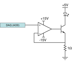
To implement a current source to drive your LED, you will be using a Darlington Transistor. This is a special device in which one transistor drives another to provide higher input-output current gain. At the LED current levels for your instrument, the TIP120 will be providing a current gain of about 500. A transistor is a three terminal device in which the voltage or current at one terminal controls the voltage across, or current through, the other two terminals. In our case, the TIP120 acts like one BJT consisting of a Base, Emitter, and Collector, and should be wired into the circuit shown in the diagram. We will use the base contact of our TIP120 to accept a small amount of current from an op-amp, which will cause the TIP120 to conduct a much larger current between it's collector and emitter, in turn allowing nearly the same level of current to flow through the LED.
As described in lecture, the op-amp will be used to linearize the behavior of the TIP120. Here the LED and transistor are inside a feedback loop extending from the output of the op-amp, through the base-emitter conduction path in the TIP120, and back from the top of the 1 Ohm resistor, whose voltage drop is thus fed-back to the negative input node of the op-amp, completing the loop. Recall that this is simply a buffer implementation, with gain of 1, where the feedback voltage is directly proportional to the LED current. Notice that in this way the current through the LED is exactly equal to the voltage applied to the op-amp positive input by the DAQ. (Remember the golden rules.)
Note: if the LED is too bright then the sample will become photobleached very quickly. In the Labview VI for Part 1, you are able to set the voltage supplied to the op-amp.
Note also that the voltage to the LED comes from the fixed 5V supply on your lab station's INSTEK GPS-3303 power supply, modulated by the TIP120, whereas the op-amp operates on +/– VCC (+/-15V in your setup).
Heating control
We will use a thermoelectic cooler (TEC) to heat the sample in this lab. A TEC is a device that becomes warm on side and cold on the other side when a DC voltage is applied across it. Before heating the sample, make sure that the TEC makes good thermal contact with the heating block. If there is not good thermal contact, hot spots will develop, damaging the TEC. To ensure good contact, use the MINIMUM amount of thermal grease, and make sure that the heating block lies flat on the TEC. Wooden sticks are available in the DNA Melting drawer (far right of the prep bench) to help you apply an very thin layer.
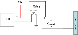
To control the TEC in this part of the lab we will use an optically isolated switch, controlled by the Labview VI for Part 1. The diagram shows the suggested schematic for the lab.
Temperature detection
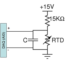
The electrical resistance of most materials varies with temperature. An RTD is a special resistor (usually made out of platinum) that exhibits a nearly linear change in its value with temperature. An RTD may be used to accurately measure temperature by including it as an element in a voltage divider. As the resistance of the RTD changes, so will the voltage across it.
A PPG102A1 RTD has been pre-mounted on the DNA heating block. This RTD has a nominal resistance of 1 kΩ and its value increases with temperature. Note that the maximum current carrying capacity of this device is 1 mA, so if you alter the voltage divider design, be sure that no more than 1 mA flows through the RTD. You can place your finger over the RTD and measure the divider voltage with a digital multimeter to test your circuit.
The diagram to the right shows the suggested circuit. The capacitor across the RTD implements a low pass filter whose purpose is to eliminate noise in your temperature reading. Consider the following points when choosing a capacitor value: What is the frequency range that you want filtered? Or, what is the time constant of the temperature change in your experiment? What is the time constant of your filter? If it is too large compared to the rate of change of temperature, it could cause a delay in your temperature reading.
Photodiode signal amplification
Excited SYBR Green I molecules emit photons in all directions, some of which pass through the aperture in the heating block then the emission filter and then strike the photodiode. This generates a tiny current in the phootdiode, which must be converted to a voltage and amplified to a level that can be conveniently measured. From past experience, the photodiode output current will be on the order of 15 nA but depends on excitation light flux and emission collection optics. (Can you calculate it from first principles?) You may be able to improve upon this with well-designed optics in the emission path.
The amplification circuit
The NI-DAQ interface card used in lab can digitize a voltage between positive and negative 10 Volts. A first approach to providing this voltage swing at the digitizer inputs was demonstrated in the homework: a transimpedance amplifier with a gain of approximately $ 10^8 $ V/A would produce an output of 1.5 V. (Why not simply use a resistor, and omit the op-amp?) However, implementing the photodiode amplifier in a single stage presents a number of challenges because many of the non-ideal behaviors of op amps become apparent at such high gain values. Because of this it is suggested that you implement a two-stage amplifier as shown in the figure below. Your job as circuit designers will be to fill in the appropriate feedback resistor values in order to achieve the desired gain at the output. If you have another topology in mind, feel free to discuss with your TA and/or Instructors.
Think carefully about how you want to distribute the gain of the system across the stages: how does feedback affect the noise of the amplifier? What are the dominant sources of noise in the DNA melting setup, which ones do you have most control over, and how will you control for them? Applying your knowledge of feedback and transfer functions, you should be able to determine the optimal gain configuration of each stage for lowest output noise.
Practical matters
Even with these optimizations, it will be important to keep your wiring short and neat. The amplifier and wiring will also be susceptible to physical movement, so prevent things from getting bumped during experimental runs. A note about resistors and capacitors: recall that resistors introduce thermal noise, while capacitors do not. Therefore, the optimized system will use as low resistor values as are reasonable in filters and feedback paths.
As with most amplifiers, care should be taken with lead dress, component placement and supply decoupling in order to ensure stability.
In theory, there is no difference between theory and practice. But, in practice, there is.
The universe is rife with electrical noise. Keeping the noise out of sensitive electronic instruments requires a great deal of care. Unfortunately, electronic breadboards are a poor environment in which to construct high gain amplifiers. A few simple tricks can improve things.
- Use power supply bypass capacitors. Connect a large capacitor between all supply voltages and ground. Large, electrolytic capacitors of at least 0.1 μF work well for this purpose. Electrolytic capacitors are polarized. Make sure to put them in the right direction (They may explode, but they will definitely start to smell bad.).
- Use the binding posts on the breadboard to connect your power supplies.
- Power Supplies: Use a seperate power supply for the op-amp circuits, LED driving circuit, and the heating control. Make sure to tie the 5V ground to +15V/-15V ground at the power supply. If you connect the grounds on the breadboard, there will be a potential difference between the grounds. This voltage difference is due to the large current swing of the LED driver flowing through the parasitic resistance of the breadboard.
PC Data Acquisition System
Each lab PC is equipped with a National Instruments USB-6212 or USB-6341 data acquisition (DAQ) card.
The USB-6212[2] has 16, 16-bit analog input channels which can, in sum total, accomplish 400 thousand samples per second (400kS/s). That is, if there are two channels, each one will be alternately sampled, and EACH sampled at 200kS/s. A multiplexer sequentially selects from among the 16 single-ended and 8 differential input signals. The card also supports two 16 bit analog output channels with an update rate of 250 kS/s and an output range of +/-10 V and up to +/-2 mA.
The USB-6212 also has 32 digital input/output channels and a digital ground. A 50 kΩ pull-down resistor is typically used in series with connections to these channels.
The USB-6341[3] is s little more powerful. It has 16, 16-bit analog input channels which can, in sum total, accomplish 500 thousand samples per second (500kS/s). Again, a multiplexer sequentially selects from among the 16 single-ended and 8 differential input signals. The card also supports two 16 bit analog output channels but they have an update rate of 900 kS/s and an output range of +/-10 V and up to +/-2 mA.
Finally, the USB-6341 has 24 digital input/output channels and a digital ground, as well as 4, 100 MHz counter/timers.
Summary of DAQ inputs/outputs
| Location | Signal | Ground |
|---|---|---|
| RTD | AI0+ | AI0- |
| Photodiode | AI1+ | AI1- |
| LED Driver | AO0 | AOGND |
| Relay | P1.0 | DGND |
Things to watch out for
- The DAQ has only one ADC (analog-to-digital converter), which is multiplexed between all of its analog inputs. The ADC has input limits of +/-10V. If one input is outside this range, it will get confused and give nonsensical values for all inputs. The upshot is, if either your temperature or fluorescence measurement is nonsensical, check to make sure the other one isn't feeding +15V into the DAQ.
- If you short-circuit your DAQ, it will get confused. One symptom of this is the LabView VI refusing to run (for example, wrongly complaining that the limits on the band-pass filter do not satisfy some condition). If this happens, unplug and re-plug the DAQ and use the Measurement and Automation software to check its condition.
LabVIEW VI
The DNA Melting LabVIEW VI is located in the Students/Labs/DNA Melting folder of the course locker. Double click to launch the VI. (The current version is R1.0)
Click the run arrow or select Operate->Run from the menu to start the VI. The top two charts show the digitized voltage at the RTD and diode inputs over time. Use the range settings to get a good view of the signal.
At the end of an experimental run, use the Save Data button to save the most recent result in a tab-delimited file that can be read into Matlab or Excel.
Debugging the apparatus
- Use freeze spray and the heat gun to make sure the temperature circuit is working properly.
- Cover and uncover the photodiode to verify operation of the fluorescence measurement system.
- Use a box and a piece of black cloth to shield your apparatus from ambient light. Can you measure the difference between a cuvette filed with water and one with DNA and SYBR Green?
- Observe every electrical signal node with the oscilloscope. Are any signals noisy? Is there a way to improve the quality of poor signals?
- Watch the fluorescence readout over time. Is it stable or does it drift?
- Is your temperature reading nonsensical? Make sure you are using 15V supply and 15kohm resistor, for your voltage supply. Also make sure that the DAQ input is placed across the RTD not the 15Kohm resistor.
- Is your LED being driven at the desired carrier frequency? Try turning the carrier frequency down low enough to see it turn on and off (try 5Hz). Try pointing the LED directly at the photodiode. Is the frequency of the photodiode signal what you expect?
- Is your sampling photobleaching quickly? Turn the amplitude of the LED signal down at the Labview VI. Try an amplitude of 0.25 V and an offset 0.50 V. Turning the amplitude down decreases signal strength, but you can gain signal strength by focusing the green fluorescent light on the photodiode with lenses.
Experimental procedure
Samples are in limited supply, as usual, so to receive your test samples you must first confirm that your apparatus is functioning properly and that your analysis script is functional. Your group can actually get your code running at the same time as your instrument is being created. You may either generate some data from the Simulating DNA melting wiki page, or you may use previous-run data that we provided on Stellar.
To demonstrate a properly running instrument, your TA will provide a sample of 20bp DNA and will evaluate your raw data. As a first step, turn your apparatus on and measure the difference between a cool DNA sample and water. Run the DNA melting LabVIEW VI in the DNAMelting directory of the course locker (First make a copy for yourself in your directory.).
Once your instrument is running to your (and your TA's) satisfaction, you may measure melting curves of each of the test samples. And if you have time, you can run additional experiments. For example, you could gather additional ionic strength data points.
The DNA melting apparatus will generate the best data when both the amplifier circuit and LED have been on for a while and all the components have reached their steady state temperature. Make sure the outputs of the system are stable before you begin taking data.
The steps for each experimental run are:
- Open the LabView VI
- Set the carrier frequency, the LED amplitude, the desired temperature, and the filter cutoff frequencies
- Then prepare a sample and place cuvette in heating block
- Run the Labview: recording RTD and photodiode output during heating
- Switch off the heater and record RTD and photodiode output during cooling
- Make any modifications to the code that will help you
Make a sample
Pipet 500μl of DNA plus dye solution into a glass cuvette. (Ask your TA or an Instructor for one of these reusable, and expensive, cuvettes). Pipet 20μl of mineral oil on top of the sample to help prevent evaporation. Put a disposable top (available in a drawer under the bench) on the cuvette and mark it with a permanent marker. Keep the sample vertical to make sure the oil stays on top. You should be able to use the same sample for several heating/cooling cycles (What makes it go bad? What can you do to limit this effect?). Only discard it if you lose significant volume due to evaporation or your signal gets too low. If you need to leave the sample overnight, store it in the lab refrigerator. If you finish with a sample and it is still in good shape, pass it on to another group.
Sample Disposal
Data Analysis
Lam Manual:Processing DNA Melting Data
References
- ↑ Zipper H, Brunner H, Bernhagen J, Vitzthum F. Investigations on DNA Intercalation and Surface Binding by SYBR Green I, its Structure Determination and Methodological Implications. Nucleic Acids Res. 2004;32:e103–10.
- ↑ Datasheet for the USB-6212
- ↑ Datasheet for the USB-6341

