Difference between revisions of "DNA Melting Part 1: Measuring Temperature and Fluorescence"
Steven Nagle (Talk | contribs) |
Juliesutton (Talk | contribs) m (→Wire the Peltier device and test it) |
||
| (309 intermediate revisions by 8 users not shown) | |||
| Line 3: | Line 3: | ||
{{Template:20.309}} | {{Template:20.309}} | ||
| − | + | <center> | |
| + | ''In theory, there is no difference between theory and practice. But, in practice, there is.'' | ||
| − | + | ''—[http://en.wikiquote.org/wiki/Jan_L._A._van_de_Snepscheut Jan L. A. van de Snepscheut]/[http://en.wikiquote.org/wiki/Yogi_Berra Yogi Berra]/and or [http://c2.com/cgi/wiki?DifferenceBetweenTheoryAndPractice Chuck Reid]'' | |
| − | + | </center> | |
| − | + | ||
| − | + | ||
| − | + | ||
| − | + | ||
| − | + | <br /> | |
| + | <br /> | ||
| − | + | ==Overview of part 1== | |
| + | [[Image:Normalized DNA melting curve.gif|thumb|right|386 px|Normalized DNA melting curve. (Plot from [http://www.gene-quantification.de/hrm-dyes.html gene-quantification.de] )]] | ||
| + | In this part of the lab, you will construct a crude version of a temperature-cycling fluorometer and measure a DNA melting curve or two. Even though this first version of the instrument has some shortcomings, it will give you a good idea of how all of the parts work together to make melting curves. The instrument includes a resistance temperature detector (RTD) to measure the temperature of the sample holder, a blue LED to excite the sample, a Peltier device that will heat the sample, optical filters, a photodiode for detecting fluorescent emission, a high-gain transimpedance amplifier to convert photocurrent to voltage, and a computer data acquisition system to record the voltages that come out of the instrument. | ||
| − | + | When you get it all put together, the instrument will produce two voltages: one related to the sample temperature and another that depends on the amount of fluorescence coming out of the sample. The goal of part 1 is to produce at least one reasonable quality melting curve. This involves recording the temperature and fluorescence voltage as you heat a sample of DNA + dye from room temperature to about 95°C and then let it cool back down. Computer software for recording the voltages has already been written for you. After you have a melting curve, you will use nonlinear regression to fit thermodynamic parameters to your data and do a little planning for part 2 of this lab. You will probably notice some shortcomings your instrument as you work. Don't worry about that — in part 2, you will make many improvements to your machine that will make it [https://youtu.be/3rQEbQJx5Bo sing like Elvis]. | |
| − | + | There are instructions below for assembling your DNA melter. | |
| − | == | + | ==Before you get started in the lab …== |
| + | Two parts of the DNA melter require you to do some design work. You will have to decide what lenses (if any) you would like to use in your system and you will also need to select component values for your transimpedance amplifier. Come up with at least a preliminary design both of these before you start building. | ||
| − | + | ===Excitation and emission optics=== | |
| + | It's possible to build a DNA melter with no lenses at all. Most people find that they can get a better signal-to-noise ratio if they use lenses. The goal is to get as much of the light from the LED to fall on the sample as possible and to get as much of the fluorescent emission on to land on the photodiode as possible. The active area of the photodiode is 3.6 mm x 3.6 mm. Take a little time to think about what lenses you'd like to use between the LED and the sample and photodiode and the sample. It wouldn't hurt to draw a ray diagram. | ||
| − | + | ===Transimpedance amplifier=== | |
| + | [[File:Transimpedance amplifier part 1.png|thumb|right|400px|Two-stage transimpedance amplifier for converting photocurrent to voltage.]] | ||
| + | Fluorescent light from the sample falls on the photodiode and produces a photocurrent. The amount of current depends on the irradiance of the sample and the light collection efficiency of your optical system (and probably some other stuff). In most instruments, the photocurrent is around a microamp, but this number can vary up or down by a few orders of magnitude depending on the details of your optics. This small current must be amplified to a level where it can be easily measured. The voltage measurement range of the data acquisition system is ±10 V. It makes sense to shoot for an output voltage that fills most of the range of the data acquisition system. The circuit shown to the right is a two-stage amplifier which converts the photodiode current to a voltage, and amplifies this voltage. | ||
| − | + | Before you build the circuit, you will need to choose values for the resistors and capacitors to get the right amount of gain and an appropriate cutoff frequency. The following questions will guide you in selecting these components (note that these questions are very similar to PSet 3). | |
| − | + | ||
| − | + | ||
| − | + | ||
| − | + | ||
| − | = | + | <ol type = "1"> |
| − | + | <li> For the amplifier circuit shown at the above right, in what case can we ignore the effect of the capacitor? At high or low frequencies? </li> | |
| + | <li> Stage 1 of the circuit (shown below) is a transimpedance amplifier, which converts the current coming from your photodiode into a voltage. Ignoring the effect of the capacitor for now (for the case you described in the above question), write an expression for the gain (<math>V_1/i_{in}</math>) of Stage 1 of your amplifier circuit in terms of the resistor values. | ||
| + | [[File:Transimpedance_Stage1_NoCap.png|thumb|center|220px|Stage 1.]] </li> | ||
| + | <li> Let’s look at Stage 2 of the amplifier circuit. This stage is a voltage amplifier to further amplify the signal from Stage 1. We need this second stage because when the gain of a single stage is very high (~10<sup>6</sup> Ω), the circuit starts to misbehave. At very high gains, you can't ignore the nonidealities of the op amp as casually as you can at low gains. Thus, to achieve an adequate gain, we need the second stage of amplification. What is the gain (<math>V_2/V_1</math>) of Stage 2? | ||
| + | [[File:Transimpedance_Stage2.png|thumb|center|200px|Stage 2.]] </li> | ||
| + | <li> Now that you know the gain of each stages of your amplifier circuit. Pick resistor values such that 1uA current from your photodiode will produce ~10V signal at the final output of the circuit (<math>V_2</math>). Remember that it is best to put as much gain in early stages of a multi-stage amplifier as possible. Since you won’t know the exact current values from your photodiode until you build your system, you will start with these values and adjust them as necessary after you build it. </li> | ||
| + | <li> It is now time to reconsider the capacitor in Stage 1 of the amplifier circuit. What does this capacitor do at high frequencies? What kind of filter is this? Using impedance analysis, find the gain (<math>V_1/i_{in}</math>) of Stage 1 in terms of the capacitor and resistor values. </li> | ||
| + | <li> What value capacitor will you choose to filter out 60 Hz and 120 Hz noise from the lab? </li> | ||
| + | </ol> | ||
| − | + | ==Assembling the system== | |
| − | + | If you have forgotten your way around the lab, consult the [[Lab orientation]] page. | |
| − | + | ||
| − | + | ||
| − | + | ||
| − | + | ||
| − | + | ||
| − | + | ||
| − | + | ||
| − | + | ||
| − | + | ||
| − | + | ||
| − | + | ||
| − | + | ||
| − | + | ||
| − | + | Start by mounting all of the main structural components on an optical breadboard. Onward! | |
| − | + | ||
| − | + | ||
| − | + | ||
| − | + | ||
| − | + | ||
| − | + | ||
| − | + | ||
| − | + | ||
| − | + | ||
| − | + | ||
| − | + | ||
| − | + | ||
| − | + | ||
| − | + | ||
| − | + | ||
| − | + | ||
| − | + | ||
| − | + | ||
| − | + | ||
| − | + | ||
| − | === | + | ===Mount the DNA melting chassis on an optical breadboard=== |
| − | + | <gallery widths=216px caption="Stuff you need:"> | |
| − | + | File:DNA melting chassis.jpg|1 DNA melting chassis (on top of Center Cabinets) | |
| + | File:Optical breadboard.jpg|1 aluminum optical breadboard (1 foot by 2 foot, part number MB1224, located in the Instructor Cubbies) | ||
| + | File:Quarter twenty by half screws.jpg|4 ¼-20x½" screws | ||
| + | File:Three wire nuts.jpg|3 wire nuts (DNA melting drawer — rightmost drawer on the wet bench.) | ||
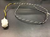
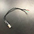
| + | File:DNA_part_1_TEC_wire_assembly.jpg| TEC extension wire assembly (on top of Center Cabinets) | ||
| + | </gallery> | ||
| − | + | The chassis includes a support bracket, fan, heat sink, and sample holder. There are two Peltier devices sandwiched between the holder and the heat sink. When current is applied to the Peltier device, the sample block will either heat up or cool down, depending on the direction of the current. There is a temperature sensor embedded inside the sample holder. | |
| − | + | # Mount the chassis on the optical breadboard using the ¼-20x5½" screws. | |
| + | #* Leave room for your optical setup and an electronic breadboard. | ||
| − | + | ===Wire the Peltier device and test it=== | |
| − | + | [[Image:Diablotek switching power supply.jpg|thumb|right|Diablotek switching power supply (inside east cabinet) provides power to the Peltier devices.]] | |
| − | + | Heating and cooling the sample with a Peltier device requires a lot of current. In part 1 of the lab, you will hook the Peltier device (also called a thermoelectric cooler, or TEC) directly to its own power supply. When you turn the power supply on, the sample will heat up. After you turn the supply off, the sample will return to room temperature by radiation, conduction, and convection — all that heat stuff. This is a pretty crude way to control the sample temperature. We'll come up with something better in part 2. | |
| − | + | ||
| − | + | ||
| − | + | ||
| − | + | ||
| − | + | ||
| − | + | ||
| − | + | ||
| − | + | ||
| − | + | ||
| − | + | ||
| − | + | ||
| − | + | ||
| − | + | ||
| − | + | ||
| − | + | ||
| − | + | [[Image:DNA part 1 TEC hookup.jpg|thumb|right|Power supply connected to Peltier devices (TECs).]] | |
| + | # Hook up the Peltier devices (TECs) in series. | ||
| + | #* There are two Peltier devices (TECs) sandwiched between the sample holder and the heat sink. | ||
| + | #* They must be connected in series. | ||
| + | #* The black lead of the top device should be connected to the red lead of the bottom device. | ||
| + | #* If these two wires are not already connected, twist them together and secure the connection with a wiring nut. | ||
| + | # Connect the TEC to the power supply | ||
| + | #* Use the TEC extension wire assembly (the correct one has black/white/black/yellow colored wires) | ||
| + | #* Join the white wire to the red lead of the top TEC and the black wire to the black lead on the bottom TEC using wire nuts. | ||
| + | # Warning: there are two connectors on the Diablotek power supply that the connector on the TEC extension wire can fit into. Make sure to use the '''black''' connector, not the white one. | ||
| + | #* Connect the TEC extension to the '''black''' connector on the Diablotek power supply. | ||
| + | # Test the TECs by touching the base of your heating block and turning the Diablotek on. | ||
| + | #* The base should start to feel warm within 10-15 seconds. | ||
| + | #* If the power supply immediately shuts off (the fan inside the power supply stops spinning) it is likely that you either used the wrong connector or there is a short circuit. Double check your wiring. | ||
| − | + | ===Measure temperature=== | |
| − | + | <gallery widths=216px caption="Stuff you need:"> | |
| − | + | File:Electronic breadboard.jpg|1 electronic breadboard (on top of east cabinet) | |
| − | + | File:CL5 clamps.jpg|2 CL5 clamps (on top of center cabinet) | |
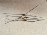
| − | + | File:15 KOhm resistor.jpg|15 KΩ resistor | |
| − | + | File:Jump wires.jpg|jump wires (on top of east cabinet) | |
| − | + | File:Banana cables.jpg|3 banana cables — preferably two red and one black or three different colors | |
| − | + | </gallery> | |
| − | + | ||
| − | + | ||
| − | + | ||
| − | + | ||
| − | + | ||
| − | + | ||
| − | + | A platinum RTD is embedded inside the heating block. The resistance of the RTD varies with temperature according to the equation ''R<sub>RTD</sub>''=1000 Ω + 3.85 ''θ'', where ''θ'' is the temperature of the RTD in degrees Celsius. | |
| − | + | ||
| − | + | ||
| − | + | ||
| − | + | # While the output is off, set the power supply to 15 V and 0.1A (SERIES operation) and connect to the breadboard. | |
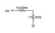
| + | # Connect the 15kΩ resistor in series with the RTD on the breadboard as shown in the diagram. [[Image: DNA_Lab_RTD_circuit.png|thumb|right|RTD circuit]] | ||
| + | #* The maximum current of the RTD is 1 mA. Since you will use a 15 V supply to the circuit, the resistor must be at least 14 kΩ. | ||
| + | #* Measure the actual resistance of the 15 kΩ resistor with a DMM and record the value in your lab report. | ||
| + | # Making sure your circuit is powered and grounded properly, turn on the output of the power supply. | ||
| + | #* Make note of the actual supply voltage measured by your DMM. | ||
| + | #* Measure the voltage across the RTD using the DMM. | ||
| + | # You may mount your electronic breadboard to your optical breadboard using the CL5 clamps, along with some screws and washers, as shown in right image. [[Image: CL5clamp.JPG|thumb|right|Clamp usage]] | ||
| − | + | * Find an equation for the voltage across the RTD as a function of temperature. What voltage do you expect given an input voltage of 15 V with the RTD at room temperature? | |
| + | * What is the measured voltage of the RTD at room temperature and how does it compare to your predictions above? | ||
| + | * What is the temperature, based on your measured voltage and how does it compare with the clock on the wall (or some better measure)? | ||
| + | * How is the temperature calculation affected by a 1% change in the 15 V input voltage? In other words, if you assume the same measured voltage across the RTD, but have a 1% change in the input voltage, how much does your calculated temperature change? Note the importance of keeping track of your input voltage. | ||
| − | ==== | + | ===Excite the sample with blue light=== |
| + | <figure id="fig:DNA_LED_circuit_part_1">[[File:DNA_LED_Circuit_part_1.svg|thumb|right|50 px|<caption>Schematic diagram of LED circuit</caption>]]</figure> | ||
| + | The circuit for illuminating the sample is pretty simple — just a blue LED in series with a resistor, powered by the 15 V supply. The circuit is shown in <xr id="fig:DNA_LED_circuit_part_1"/>. In this connection, the LED will shine with a roughly constant intensity. This part of the circuit will more complicated in part 2. For part 1, a constant, blue light source will do the trick. | ||
| − | + | Light coming out of the LED diverges pretty quickly. You might be able to get more light to fall on the sample with a lens. | |
| − | + | <gallery widths=216px caption="Stuff you need:"> | |
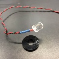
| − | + | File:Blue LED with mounting ring.jpg|1 blue LED with mounting ring (rightmost drawer of west drawers) | |
| − | + | File:62 ohm resistor.jpg|1 62 Ω resistor | |
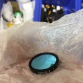
| + | File:D470 filter.jpg|1 D470/40 excitation filter (DNA melting drawer- rightmost drawer on wet bench) | ||
| + | File:SM1L05.jpg|1 ½" SM1 lens tube (on shelves) | ||
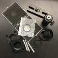
| + | File:Optical parts for excitation.jpg|lenses and mounts for excitation optical path | ||
| + | </gallery> | ||
| − | + | # Mount the LED in its mounting ring and secure it in a lens tube with a retaining ring. | |
| − | + | # Assemble your excitation optical path. | |
| − | * | + | #* LEDs have a broad emission spectrum, so it's necessary to put an optical filter between the LED and the sample. |
| − | * | + | #* The arrow on the side of the filter should point toward the sample. |
| − | + | # Use your electronic breadboard to wire the 62 Ω resistor in series with the LED, as shown in <xr id="fig:DNA_LED_circuit_part_1"/>. | |
| + | # Use banana cables to route the 5V output of the lab power supply to the LED circuit. | ||
| + | #* Don't forget to connect the resistor — if there is no resistor in series the LED will blow out. | ||
| + | # Turn on the power supply and enable the output. | ||
| + | #* If the LED doesn't glow, it's time for some debugging. | ||
| − | == | + | ===Detect green fluorescence=== |
| + | You will use a photodiode, a transimpedance amplifier, an emission filter, and possibly some lenses to detect fluorescent light from the sample. It's time to put all of that together. Start by building and testing the amplifier. Then put the optical system together. | ||
| − | == | + | ====Construct the emission optical path==== |
| + | <gallery> | ||
| + | File:SM05PD1A Photodiode.jpg|1 SM05PD1A photodiode (DNA melting drawer) | ||
| + | File:SM1A6 adapter.jpg|1 ½" to 1" adapter (DNA melting drawer) | ||
| + | File:E515LPv2 filter.jpg|1 E515LPv2 emission filter (DNA melting drawer) | ||
| + | File:Optical parts for emission.jpg|lenses and mounts for emission optical path | ||
| + | </gallery> | ||
| − | + | # Mount the photodiode in its adapter and place the whole thing inside a lens tube. | |
| + | # Mount and secure the emission optical path. Don't forget the filter (the arrow should be pointing toward the sample). | ||
| + | # Consider using a lens to focus the light emitted from your sample onto your photodiode. | ||
| − | + | ====Build the transimpedance amplifier==== | |
| − | . | + | It's time to build the transimpedance amplifier that will convert the tiny current produced by the photodiode into a measurable voltage. If you didn't already select component values, you are probably not very good at following directions. Pick component values before you start building. |
| − | . | + | |
| + | <gallery widths=216px caption="Stuff you need:"> | ||
| + | File:LF411 op amps.jpg|2 LF411 op amps (rightmost drawer of west drawers) | ||
| + | File:Resistors for transimpedance amplifier circuit.jpg|Resistors for amplifier circuit | ||
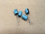
| + | File:DNA bypass capacitors.jpg|4 capacitors > 1 μF (rightmost drawer of west drawers) | ||
| + | File:SMA to BNC.jpg|1 SMA to BNC adapter (DNA melting drawer) | ||
| + | File:BNC cable.jpg|1 BNC cable | ||
| + | File:BNC to wires adapter.jpg|1 BNC wire adapter (on center cabinet) | ||
| + | </gallery> | ||
| − | + | # Disable the power supply before you start. | |
| + | # Configure the lab power supply for series mode and set the voltage to ±15 V. | ||
| + | # Use banana plugs to wire +15 V, ground, and -15 V to the breadboard terminals. | ||
| + | # Mount the two op amps a short distance apart on the electronic breadboard. The amplifiers should straddle the notch on the breadboard that separates the two sets of bus strips. | ||
| + | #* Make sure to use the correct kind of amplifier — there are several types in the drawer that look very similar. The package should say "LF411" on it. | ||
| + | #* Orient the op-amps so that pin 1 (marked with a dot on the package) is at the upper left. | ||
| + | #* Use jump wires to connect the power supplies from the breadboard terminals to the bus bars on the left and right of the op amps. | ||
| + | #** Wire the +15 V power supply to the red bus bar on the right of the op amps. | ||
| + | #** Wire the -15 V power supply to the red bus bar to the left of the op amps. | ||
| + | #** Connect the blue bus bars on either side of the amplifiers to ground. | ||
| + | #* Use short wires to connect the power pins of the op amps to the correct power supplies. Double check your connections — there is no faster way to ruin an op amp than to wire the power backwards. | ||
| + | #* Add the bypass capacitors (the blue ones in the above image) to your circuit to reduce noise from the power supply. Do this by straddling a capacitor between the +15 V supply (pin 7) to ground, and another capacitor between the -15 V supply (pin 4) to ground. Be sure to note the polarity of your capacitor (the black stripe should go toward the more negative potential) otherwise you might get an unwanted explosion. | ||
| + | # Build the transimpedance amplifier circuit with the component values you selected. [[Image: LF411.jpg|thumb|right|LF411 op amp pin configuration]] | ||
| + | # Use a SMA to BNC adapter; BNC cable; and BNC to wire adapter to connect the photodiode terminals to the electronic breadboard. | ||
| + | # Before you enable the power supply, double check that your component values are correct and your connections match the design. | ||
| + | # Test it out | ||
| + | ## Enable the power supply and verify that +15V appears on pin 7 and -15V on pin 4. | ||
| + | ## Temporarily disconnect the photodiode from the amplifier input. This will set the input current to zero. | ||
| + | ## Measure the voltage on the output pins of both amplifiers (pin 6). | ||
| + | ##* If the outputs are not close to zero (say, less than a hundred millivolts), there is probably something wrong. Time for some debugging. | ||
| + | ## Reconnect the photodiode. Hook a voltmeter to the amplifier output. | ||
| + | ## Point the photodiode at the lights. Now cover the photodiode with your thumb or another appendage. | ||
| + | ##* If the voltage doesn't change as expected, it's time for some debugging. | ||
| − | == | + | ==Connect your instrument to the computer data acquisition system== |
| − | + | ||
| − | + | ||
| − | + | ||
| − | + | ||
| − | + | ||
| − | + | ||
| − | + | ||
| − | + | ||
| − | + | ||
| − | + | ||
| − | + | ||
| − | + | ||
| − | + | ||
| − | + | ||
| − | + | ||
| − | + | ||
| − | + | ||
| − | + | ||
| − | + | ||
| − | + | ||
| − | + | ||
| − | + | ||
| − | + | ||
| − | + | ||
| − | + | ||
| − | + | ||
| − | + | ||
| − | + | ||
| − | + | ||
| − | + | ||
| − | + | ||
| − | + | ||
| − | + | ||
| − | + | ||
| − | + | ||
| − | + | ||
| − | + | ||
| − | + | ||
| − | + | ||
| − | + | ||
| − | + | ||
| − | + | ||
| − | + | ||
| − | + | ||
| − | + | ||
| − | + | ||
| − | + | ||
| − | + | ||
| − | + | ||
| − | + | ||
| − | + | ||
| − | + | ||
| − | + | ||
| − | + | ||
| − | + | ||
| − | + | ||
| − | + | ||
| − | + | ||
| − | + | ||
| − | + | ||
| − | + | ||
| − | + | ||
| − | + | ||
| − | + | ||
| − | + | ||
| − | + | ||
| − | + | ||
| − | + | ||
| − | + | ||
| − | + | ||
| − | + | ||
| − | + | ||
| − | + | ||
{{:20.309:DAQ System}} | {{:20.309:DAQ System}} | ||
| Line 256: | Line 211: | ||
<center>[[Image:DAQ_Wire_Colors.png|450 px|thumb|center|DAQ Connection Cable]]</center> | <center>[[Image:DAQ_Wire_Colors.png|450 px|thumb|center|DAQ Connection Cable]]</center> | ||
| − | == | + | ==DNAMelter software== |
| − | + | ||
| − | + | ||
| − | + | ||
| − | + | ||
| − | == | + | |
| − | + | ||
| − | + | ||
| − | + | ||
| − | + | ||
| − | + | ||
| − | + | ||
| − | + | ||
| − | + | ||
| − | + | ||
| − | + | ||
| − | + | [[Image:BasicDNAMelterIcon.png|75 px|left]] | |
| + | Use the <code>Basic DNA Melter GUI</code> program (located on the lab computer desktop) to collect data from the apparatus. | ||
| − | + | Use the "Open file ..." button to write the data to a file. The data will be tab-delimited and can be read into Matlab with the <code>load</code> command. | |
| − | + | Documentation for the DNAMelter software is available here: [[DNA Melting: Using the Basic DNAMelter GUI]] | |
| − | == | + | ====If you need to debug the DAQ (skip otherwise!)==== |
| + | * When debugging problems, it is frequently useful to ascertain whether the data acquisition system is working properly. National Instruments provides an application for this purpose called Measurement and Automation Explorer. Use Measurement and Automation Explorer to verify that the DAQ is properly connected to and communicating with the computer. The program also provides the ability to manually control all of the DAQ system's inputs and outputs. | ||
| + | ** Launch Measurement and Automation Explorer by selecting Start->All Applications->National Instruments->Measurement and Automation. | ||
| + | ** In the "Configuration" tab, select "Devices and Interfaces" and then "NI-DAQMx Devices." Select "Dev1." | ||
| + | ** If Dev 1 does not show up, the problem is that computer cannot communicate with the DAQ system. Ensure that the USB cable is connected to the DAQ system. If the cable is connected and the device still does not show up, unplug the USB cable, count to five, and plug it back in. | ||
| + | ** If the DAQ shows up under a different name, disconnect the USB cable. Delete all the "NI USB-6xxx" entries and then reconnect the USB cable. Verify that one entry reappears and that it is called "Dev1." | ||
| + | ** Select the "Test Panels" tab to manually control or read signals from the DAQ. | ||
| + | * If you run DNAMelter and there is a data acquisition error, for example, "<code>Data acquisition cannot start!</code>", open Measurement and Automation Explorer and follow the steps above. Run DNAMelter again. If it still doesn't work, grab a beer or ask an instructor for help. | ||
| + | * The DAQ has only one analog-to-digital converter (ADC). A multiplexer circuit sequentially samples voltages from the analog inputs configured in the control software. If any of the inputs is outside the allowable range of +/-10V, all of the inputs may behave erratically. The voltages reported may look reasonable so this can be very misleading. If none of the DAQ readings make sense, ensure that all of the analog voltages are in the allowable range and reset the DAQ by cycling the power of the DAQ (use the switch on the 6341 or disconnect the USB of the 6212). | ||
| + | * If the DAQ gets short-circuited, it may crash. If this happens, Matlab will frequently give a deceptive error message, for example claiming that the limits on the band-pass filter do not satisfy some condition. In this case, correct the connection and cycle the DAQ power. | ||
| − | + | ==Part 1 measurements== | |
| − | + | ||
| − | + | ||
| − | + | ||
| − | + | ||
| − | + | ||
| − | + | ||
| − | == | + | ===Test your instrument with fluorescein=== |
| + | use ~ 30μM fluorescein to test your instrument before you get started with DNA samples. Fluorescein is good for testing; it's cheap, non-toxic, and it does not bleach as quickly like LC Green. | ||
| − | + | # Pipette 500 μl of fluorescein into a glass sample vial. | |
| + | # Pipette 500 μl of DI water into a another sample vial. | ||
| + | # Alternate between the two samples. You should see a difference in the transimpedance amplifier output. | ||
| − | === | + | ===Measure signal to noise ratio=== |
| − | + | Measure the signal to noise ratio (SNR) of the instrument by comparing the difference between the average signal with a sample present and with water as a null reference. This process requires a vial containing 500 uL of 30 uM fluorescein and a vial containing the same amount of water. | |
| − | + | ||
| − | + | ||
| − | + | ||
| − | + | ||
| − | + | ||
| − | + | ||
| − | + | ||
| − | + | # Run the <code>Basic DNA Melter GUI</code>. | |
| + | # Place a vial of DI water in your instrument. | ||
| + | # Clear the data and wait 10 seconds. | ||
| + | # Replace the water vial with the DNA of fluorescein vial, record for another 10 seconds, then save the data. | ||
| + | #* Be sure that all other conditions, such as temperature, are stable throughout the test. | ||
| − | { | + | Compute the signal to noise ratio, <math>\text{SNR}=\frac{\langle V_{fluorescein} \rangle - \langle V_{water} \rangle}{\sigma_{fluorescein} }</math>, where <math>V_{fluorescein}</math> is the portion of the data recorded with a fluorescein sample, <math>V_{water}</math> is the portion of the signal corresponding to the water sample, and <math>\sigma_{fluorescein}</math> is the standard deviation of <math>V_{fluorescein}</math>. |
| − | === | + | ===Make a DNA melting curve=== |
| − | + | Once the instrument is confirmed to be functioning properly, follow these instructions to generate melting curve data for a 20 bp DNA and green dye solution. | |
| − | + | ||
| − | + | ||
| − | + | ||
| − | + | ||
| − | + | ||
| − | + | {{Template:Biohazard warning|message=LC Green in DMSO is readily absorbed through skin. Synthetic oligonucleotides may be harmful by inhalation, ingestion, or skin absorption. Wear gloves when handling samples. Wear safety goggles at all times when pipetting the LC Green/DNA samples. Do not create aerosols. The health effects of LC Green have not been thoroughly investigated. See the LC Green and synthetic oligonucleotide under <code>../EHS Guidelines/MSDS Repository</code> in the course locker for more information.}} | |
| − | + | #Pipet 500 μL of DNA plus dye solution into a glass vial. | |
| − | + | #Pipet up to 20 μL of mineral oil on top of the sample to help prevent evaporation. | |
| + | #* The oil layer will reduce evaporation. | ||
| + | #* Be careful not to get oil on the cuvette sides far above the sample. It will run down during your experiment and cause shifts in the photodiode signal. | ||
| + | #*Keep the sample vertical to make sure the oil stays on top. | ||
| + | # Make sure that the Diablotek power supply is off and the sample block is near room temperature. | ||
| + | # Place the vial in the instrument | ||
| + | #* To reduce bleaching, keep the LED off until you start the measurement. | ||
| + | # Open and run the Basic DNA Melter GUI and follow the instructions there. | ||
| + | # Confirm that sample block temperature displayed in Basic DNA Melter GUI is near room temperature. | ||
| + | # Turn on the Diablotek power supply until the block temperature reaches 95°C. | ||
| + | # Attempt to hold the temperature at 95°C for a minute or so by repeatedly switching the Diablotek power supply off and on. | ||
| + | # Switch off the power supply and allow the block to cool down to room temperature. | ||
| + | #* Be sure to save your data so you can plot it in your Part 1 report. | ||
| − | |||
| − | + | * You can use the same sample for several heating/cooling cycles. | |
| + | * Only discard a sample if you lose significant volume due to evaporation or if your signal gets too low. | ||
| − | + | To clean your glass vial between samples, flush with alcohol in the waste container and rinse with water at the drain. Suck out residual liquid with the vacuum and drawn Pasteur pipette to the left of the sink. | |
| − | + | ||
| − | + | ====Sample disposal==== | |
| − | + | {{Template:Environmental Warning|message=Discard pipette tips with DNA sample residue in the pipette tips or the ''Biohazard Sharps'' container. Do not pour synthetic oligonucleotides with LC Green down the drain. Pour your used samples into the waste container provided in the middle of the wet bench.}} | |
| − | |||
| − | |||
| − | {{ | + | {{:DNA Melting Report Requirements for Part 1}} |
==Lab manual sections== | ==Lab manual sections== | ||
| Line 353: | Line 301: | ||
==Subset of datasheets== | ==Subset of datasheets== | ||
(Many more can be found online or on the course share) | (Many more can be found online or on the course share) | ||
| − | #[http:// | + | #[http://www.ni.com/pdf/manuals/371931f.pdf National Instruments USB-6212 user manual] |
| − | #[http://www. | + | #[http://www.ni.com/pdf/manuals/370784d.pdf National Instruments USB-6341 user manual] |
#[http://www.national.com/ds/LF/LF411.pdf Op-amp datasheet] | #[http://www.national.com/ds/LF/LF411.pdf Op-amp datasheet] | ||
| − | |||
| − | |||
{{Template:20.309 bottom}} | {{Template:20.309 bottom}} | ||
Latest revision as of 17:49, 19 April 2017

In theory, there is no difference between theory and practice. But, in practice, there is.
Overview of part 1

In this part of the lab, you will construct a crude version of a temperature-cycling fluorometer and measure a DNA melting curve or two. Even though this first version of the instrument has some shortcomings, it will give you a good idea of how all of the parts work together to make melting curves. The instrument includes a resistance temperature detector (RTD) to measure the temperature of the sample holder, a blue LED to excite the sample, a Peltier device that will heat the sample, optical filters, a photodiode for detecting fluorescent emission, a high-gain transimpedance amplifier to convert photocurrent to voltage, and a computer data acquisition system to record the voltages that come out of the instrument.
When you get it all put together, the instrument will produce two voltages: one related to the sample temperature and another that depends on the amount of fluorescence coming out of the sample. The goal of part 1 is to produce at least one reasonable quality melting curve. This involves recording the temperature and fluorescence voltage as you heat a sample of DNA + dye from room temperature to about 95°C and then let it cool back down. Computer software for recording the voltages has already been written for you. After you have a melting curve, you will use nonlinear regression to fit thermodynamic parameters to your data and do a little planning for part 2 of this lab. You will probably notice some shortcomings your instrument as you work. Don't worry about that — in part 2, you will make many improvements to your machine that will make it sing like Elvis.
There are instructions below for assembling your DNA melter.
Before you get started in the lab …
Two parts of the DNA melter require you to do some design work. You will have to decide what lenses (if any) you would like to use in your system and you will also need to select component values for your transimpedance amplifier. Come up with at least a preliminary design both of these before you start building.
Excitation and emission optics
It's possible to build a DNA melter with no lenses at all. Most people find that they can get a better signal-to-noise ratio if they use lenses. The goal is to get as much of the light from the LED to fall on the sample as possible and to get as much of the fluorescent emission on to land on the photodiode as possible. The active area of the photodiode is 3.6 mm x 3.6 mm. Take a little time to think about what lenses you'd like to use between the LED and the sample and photodiode and the sample. It wouldn't hurt to draw a ray diagram.
Transimpedance amplifier
Fluorescent light from the sample falls on the photodiode and produces a photocurrent. The amount of current depends on the irradiance of the sample and the light collection efficiency of your optical system (and probably some other stuff). In most instruments, the photocurrent is around a microamp, but this number can vary up or down by a few orders of magnitude depending on the details of your optics. This small current must be amplified to a level where it can be easily measured. The voltage measurement range of the data acquisition system is ±10 V. It makes sense to shoot for an output voltage that fills most of the range of the data acquisition system. The circuit shown to the right is a two-stage amplifier which converts the photodiode current to a voltage, and amplifies this voltage.
Before you build the circuit, you will need to choose values for the resistors and capacitors to get the right amount of gain and an appropriate cutoff frequency. The following questions will guide you in selecting these components (note that these questions are very similar to PSet 3).
- For the amplifier circuit shown at the above right, in what case can we ignore the effect of the capacitor? At high or low frequencies?
- Stage 1 of the circuit (shown below) is a transimpedance amplifier, which converts the current coming from your photodiode into a voltage. Ignoring the effect of the capacitor for now (for the case you described in the above question), write an expression for the gain ($ V_1/i_{in} $) of Stage 1 of your amplifier circuit in terms of the resistor values.
 Stage 1.
- Let’s look at Stage 2 of the amplifier circuit. This stage is a voltage amplifier to further amplify the signal from Stage 1. We need this second stage because when the gain of a single stage is very high (~106 Ω), the circuit starts to misbehave. At very high gains, you can't ignore the nonidealities of the op amp as casually as you can at low gains. Thus, to achieve an adequate gain, we need the second stage of amplification. What is the gain ($ V_2/V_1 $) of Stage 2?
 Stage 2.
 - Now that you know the gain of each stages of your amplifier circuit. Pick resistor values such that 1uA current from your photodiode will produce ~10V signal at the final output of the circuit ($ V_2 $). Remember that it is best to put as much gain in early stages of a multi-stage amplifier as possible. Since you won’t know the exact current values from your photodiode until you build your system, you will start with these values and adjust them as necessary after you build it.
- It is now time to reconsider the capacitor in Stage 1 of the amplifier circuit. What does this capacitor do at high frequencies? What kind of filter is this? Using impedance analysis, find the gain ($ V_1/i_{in} $) of Stage 1 in terms of the capacitor and resistor values.
- What value capacitor will you choose to filter out 60 Hz and 120 Hz noise from the lab?
Assembling the system
If you have forgotten your way around the lab, consult the Lab orientation page.
Start by mounting all of the main structural components on an optical breadboard. Onward!
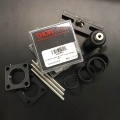
Mount the DNA melting chassis on an optical breadboard
- Stuff you need:
1 DNA melting chassis (on top of Center Cabinets)
1 aluminum optical breadboard (1 foot by 2 foot, part number MB1224, located in the Instructor Cubbies)
4 ¼-20x½" screws
3 wire nuts (DNA melting drawer — rightmost drawer on the wet bench.)
TEC extension wire assembly (on top of Center Cabinets)


The chassis includes a support bracket, fan, heat sink, and sample holder. There are two Peltier devices sandwiched between the holder and the heat sink. When current is applied to the Peltier device, the sample block will either heat up or cool down, depending on the direction of the current. There is a temperature sensor embedded inside the sample holder.
- Mount the chassis on the optical breadboard using the ¼-20x5½" screws.
- Leave room for your optical setup and an electronic breadboard.
Wire the Peltier device and test it

Heating and cooling the sample with a Peltier device requires a lot of current. In part 1 of the lab, you will hook the Peltier device (also called a thermoelectric cooler, or TEC) directly to its own power supply. When you turn the power supply on, the sample will heat up. After you turn the supply off, the sample will return to room temperature by radiation, conduction, and convection — all that heat stuff. This is a pretty crude way to control the sample temperature. We'll come up with something better in part 2.

- Hook up the Peltier devices (TECs) in series.
- There are two Peltier devices (TECs) sandwiched between the sample holder and the heat sink.
- They must be connected in series.
- The black lead of the top device should be connected to the red lead of the bottom device.
- If these two wires are not already connected, twist them together and secure the connection with a wiring nut.
- Connect the TEC to the power supply
- Use the TEC extension wire assembly (the correct one has black/white/black/yellow colored wires)
- Join the white wire to the red lead of the top TEC and the black wire to the black lead on the bottom TEC using wire nuts.
- Warning: there are two connectors on the Diablotek power supply that the connector on the TEC extension wire can fit into. Make sure to use the black connector, not the white one.
- Connect the TEC extension to the black connector on the Diablotek power supply.
- Test the TECs by touching the base of your heating block and turning the Diablotek on.
- The base should start to feel warm within 10-15 seconds.
- If the power supply immediately shuts off (the fan inside the power supply stops spinning) it is likely that you either used the wrong connector or there is a short circuit. Double check your wiring.
Measure temperature
- Stuff you need:
1 electronic breadboard (on top of east cabinet)
2 CL5 clamps (on top of center cabinet)
15 KΩ resistor
jump wires (on top of east cabinet)
3 banana cables — preferably two red and one black or three different colors


A platinum RTD is embedded inside the heating block. The resistance of the RTD varies with temperature according to the equation RRTD=1000 Ω + 3.85 θ, where θ is the temperature of the RTD in degrees Celsius.
- While the output is off, set the power supply to 15 V and 0.1A (SERIES operation) and connect to the breadboard.
- Connect the 15kΩ resistor in series with the RTD on the breadboard as shown in the diagram.
 RTD circuit
- The maximum current of the RTD is 1 mA. Since you will use a 15 V supply to the circuit, the resistor must be at least 14 kΩ.
- Measure the actual resistance of the 15 kΩ resistor with a DMM and record the value in your lab report.
- Making sure your circuit is powered and grounded properly, turn on the output of the power supply.
- Make note of the actual supply voltage measured by your DMM.
- Measure the voltage across the RTD using the DMM.
- You may mount your electronic breadboard to your optical breadboard using the CL5 clamps, along with some screws and washers, as shown in right image.
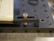 Clamp usage


- Find an equation for the voltage across the RTD as a function of temperature. What voltage do you expect given an input voltage of 15 V with the RTD at room temperature?
- What is the measured voltage of the RTD at room temperature and how does it compare to your predictions above?
- What is the temperature, based on your measured voltage and how does it compare with the clock on the wall (or some better measure)?
- How is the temperature calculation affected by a 1% change in the 15 V input voltage? In other words, if you assume the same measured voltage across the RTD, but have a 1% change in the input voltage, how much does your calculated temperature change? Note the importance of keeping track of your input voltage.
Excite the sample with blue light

The circuit for illuminating the sample is pretty simple — just a blue LED in series with a resistor, powered by the 15 V supply. The circuit is shown in Figure 1. In this connection, the LED will shine with a roughly constant intensity. This part of the circuit will more complicated in part 2. For part 1, a constant, blue light source will do the trick.
Light coming out of the LED diverges pretty quickly. You might be able to get more light to fall on the sample with a lens.
- Stuff you need:
1 blue LED with mounting ring (rightmost drawer of west drawers)
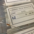
1 62 Ω resistor
1 D470/40 excitation filter (DNA melting drawer- rightmost drawer on wet bench)
1 ½" SM1 lens tube (on shelves)
lenses and mounts for excitation optical path


- Mount the LED in its mounting ring and secure it in a lens tube with a retaining ring.
- Assemble your excitation optical path.
- LEDs have a broad emission spectrum, so it's necessary to put an optical filter between the LED and the sample.
- The arrow on the side of the filter should point toward the sample.
- Use your electronic breadboard to wire the 62 Ω resistor in series with the LED, as shown in Figure 1.
- Use banana cables to route the 5V output of the lab power supply to the LED circuit.
- Don't forget to connect the resistor — if there is no resistor in series the LED will blow out.
- Turn on the power supply and enable the output.
- If the LED doesn't glow, it's time for some debugging.
Detect green fluorescence
You will use a photodiode, a transimpedance amplifier, an emission filter, and possibly some lenses to detect fluorescent light from the sample. It's time to put all of that together. Start by building and testing the amplifier. Then put the optical system together.
Construct the emission optical path
1 SM05PD1A photodiode (DNA melting drawer)
1 ½" to 1" adapter (DNA melting drawer)
1 E515LPv2 emission filter (DNA melting drawer)
lenses and mounts for emission optical path


- Mount the photodiode in its adapter and place the whole thing inside a lens tube.
- Mount and secure the emission optical path. Don't forget the filter (the arrow should be pointing toward the sample).
- Consider using a lens to focus the light emitted from your sample onto your photodiode.
Build the transimpedance amplifier
It's time to build the transimpedance amplifier that will convert the tiny current produced by the photodiode into a measurable voltage. If you didn't already select component values, you are probably not very good at following directions. Pick component values before you start building.
- Stuff you need:
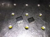
2 LF411 op amps (rightmost drawer of west drawers)
Resistors for amplifier circuit
4 capacitors > 1 μF (rightmost drawer of west drawers)
1 SMA to BNC adapter (DNA melting drawer)
1 BNC cable
1 BNC wire adapter (on center cabinet)


- Disable the power supply before you start.
- Configure the lab power supply for series mode and set the voltage to ±15 V.
- Use banana plugs to wire +15 V, ground, and -15 V to the breadboard terminals.
- Mount the two op amps a short distance apart on the electronic breadboard. The amplifiers should straddle the notch on the breadboard that separates the two sets of bus strips.
- Make sure to use the correct kind of amplifier — there are several types in the drawer that look very similar. The package should say "LF411" on it.
- Orient the op-amps so that pin 1 (marked with a dot on the package) is at the upper left.
- Use jump wires to connect the power supplies from the breadboard terminals to the bus bars on the left and right of the op amps.
- Wire the +15 V power supply to the red bus bar on the right of the op amps.
- Wire the -15 V power supply to the red bus bar to the left of the op amps.
- Connect the blue bus bars on either side of the amplifiers to ground.
- Use short wires to connect the power pins of the op amps to the correct power supplies. Double check your connections — there is no faster way to ruin an op amp than to wire the power backwards.
- Add the bypass capacitors (the blue ones in the above image) to your circuit to reduce noise from the power supply. Do this by straddling a capacitor between the +15 V supply (pin 7) to ground, and another capacitor between the -15 V supply (pin 4) to ground. Be sure to note the polarity of your capacitor (the black stripe should go toward the more negative potential) otherwise you might get an unwanted explosion.
- Build the transimpedance amplifier circuit with the component values you selected.
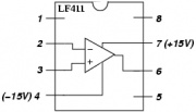 LF411 op amp pin configuration
 - Use a SMA to BNC adapter; BNC cable; and BNC to wire adapter to connect the photodiode terminals to the electronic breadboard.
- Before you enable the power supply, double check that your component values are correct and your connections match the design.
- Test it out
- Enable the power supply and verify that +15V appears on pin 7 and -15V on pin 4.
- Temporarily disconnect the photodiode from the amplifier input. This will set the input current to zero.
- Measure the voltage on the output pins of both amplifiers (pin 6).
- If the outputs are not close to zero (say, less than a hundred millivolts), there is probably something wrong. Time for some debugging.
- Reconnect the photodiode. Hook a voltmeter to the amplifier output.
- Point the photodiode at the lights. Now cover the photodiode with your thumb or another appendage.
- If the voltage doesn't change as expected, it's time for some debugging.

Connect your instrument to the computer data acquisition system
Each lab PC is equipped with a National Instruments USB-6212 or USB-6341 data acquisition (DAQ) card.
The USB-6212[1] has 16, 16-bit analog input channels which can, in sum total, accomplish 400 thousand samples per second (400kS/s). That is, if there are two channels, each one will be alternately sampled, and EACH sampled at 200kS/s. A multiplexer sequentially selects from among the 16 single-ended and 8 differential input signals. The card also supports two 16 bit analog output channels with an update rate of 250 kS/s and an output range of +/-10 V and up to +/-2 mA.
The USB-6212 also has 32 digital input/output channels and a digital ground. A 50 kΩ pull-down resistor is typically used in series with connections to these channels.
The USB-6341[2] is s little more powerful. It has 16, 16-bit analog input channels which can, in sum total, accomplish 500 thousand samples per second (500kS/s). Again, a multiplexer sequentially selects from among the 16 single-ended and 8 differential input signals. The card also supports two 16 bit analog output channels but they have an update rate of 900 kS/s and an output range of +/-10 V and up to +/-2 mA.
Finally, the USB-6341 has 24 digital input/output channels and a digital ground, as well as 4, 100 MHz counter/timers.
Summary of DAQ inputs/outputs
A special connector has been prepared for you, connected as shown below. The connections and cable wire colors are also summarized in a memo.
| Signal Name | Signal Location | Ground Location | Pin wire color |
|---|---|---|---|
| DAQ Inputs | |||
| RTD | AI0+ | AI0- | +Orange / -Black [lone pair, not with third (red) wire] |
| Photodiode | AI1+ | AI1- | +Green / -White |

DNAMelter software

Use the Basic DNA Melter GUI program (located on the lab computer desktop) to collect data from the apparatus.
Use the "Open file ..." button to write the data to a file. The data will be tab-delimited and can be read into Matlab with the load command.
Documentation for the DNAMelter software is available here: DNA Melting: Using the Basic DNAMelter GUI
If you need to debug the DAQ (skip otherwise!)
- When debugging problems, it is frequently useful to ascertain whether the data acquisition system is working properly. National Instruments provides an application for this purpose called Measurement and Automation Explorer. Use Measurement and Automation Explorer to verify that the DAQ is properly connected to and communicating with the computer. The program also provides the ability to manually control all of the DAQ system's inputs and outputs.
- Launch Measurement and Automation Explorer by selecting Start->All Applications->National Instruments->Measurement and Automation.
- In the "Configuration" tab, select "Devices and Interfaces" and then "NI-DAQMx Devices." Select "Dev1."
- If Dev 1 does not show up, the problem is that computer cannot communicate with the DAQ system. Ensure that the USB cable is connected to the DAQ system. If the cable is connected and the device still does not show up, unplug the USB cable, count to five, and plug it back in.
- If the DAQ shows up under a different name, disconnect the USB cable. Delete all the "NI USB-6xxx" entries and then reconnect the USB cable. Verify that one entry reappears and that it is called "Dev1."
- Select the "Test Panels" tab to manually control or read signals from the DAQ.
- If you run DNAMelter and there is a data acquisition error, for example, "
Data acquisition cannot start!", open Measurement and Automation Explorer and follow the steps above. Run DNAMelter again. If it still doesn't work, grab a beer or ask an instructor for help. - The DAQ has only one analog-to-digital converter (ADC). A multiplexer circuit sequentially samples voltages from the analog inputs configured in the control software. If any of the inputs is outside the allowable range of +/-10V, all of the inputs may behave erratically. The voltages reported may look reasonable so this can be very misleading. If none of the DAQ readings make sense, ensure that all of the analog voltages are in the allowable range and reset the DAQ by cycling the power of the DAQ (use the switch on the 6341 or disconnect the USB of the 6212).
- If the DAQ gets short-circuited, it may crash. If this happens, Matlab will frequently give a deceptive error message, for example claiming that the limits on the band-pass filter do not satisfy some condition. In this case, correct the connection and cycle the DAQ power.
Part 1 measurements
Test your instrument with fluorescein
use ~ 30μM fluorescein to test your instrument before you get started with DNA samples. Fluorescein is good for testing; it's cheap, non-toxic, and it does not bleach as quickly like LC Green.
- Pipette 500 μl of fluorescein into a glass sample vial.
- Pipette 500 μl of DI water into a another sample vial.
- Alternate between the two samples. You should see a difference in the transimpedance amplifier output.
Measure signal to noise ratio
Measure the signal to noise ratio (SNR) of the instrument by comparing the difference between the average signal with a sample present and with water as a null reference. This process requires a vial containing 500 uL of 30 uM fluorescein and a vial containing the same amount of water.
- Run the
Basic DNA Melter GUI. - Place a vial of DI water in your instrument.
- Clear the data and wait 10 seconds.
- Replace the water vial with the DNA of fluorescein vial, record for another 10 seconds, then save the data.
- Be sure that all other conditions, such as temperature, are stable throughout the test.
Compute the signal to noise ratio, $ \text{SNR}=\frac{\langle V_{fluorescein} \rangle - \langle V_{water} \rangle}{\sigma_{fluorescein} } $, where $ V_{fluorescein} $ is the portion of the data recorded with a fluorescein sample, $ V_{water} $ is the portion of the signal corresponding to the water sample, and $ \sigma_{fluorescein} $ is the standard deviation of $ V_{fluorescein} $.
Make a DNA melting curve
Once the instrument is confirmed to be functioning properly, follow these instructions to generate melting curve data for a 20 bp DNA and green dye solution.
| |
LC Green in DMSO is readily absorbed through skin. Synthetic oligonucleotides may be harmful by inhalation, ingestion, or skin absorption. Wear gloves when handling samples. Wear safety goggles at all times when pipetting the LC Green/DNA samples. Do not create aerosols. The health effects of LC Green have not been thoroughly investigated. See the LC Green and synthetic oligonucleotide under ../EHS Guidelines/MSDS Repository in the course locker for more information.
|
- Pipet 500 μL of DNA plus dye solution into a glass vial.
- Pipet up to 20 μL of mineral oil on top of the sample to help prevent evaporation.
- The oil layer will reduce evaporation.
- Be careful not to get oil on the cuvette sides far above the sample. It will run down during your experiment and cause shifts in the photodiode signal.
- Keep the sample vertical to make sure the oil stays on top.
- Make sure that the Diablotek power supply is off and the sample block is near room temperature.
- Place the vial in the instrument
- To reduce bleaching, keep the LED off until you start the measurement.
- Open and run the Basic DNA Melter GUI and follow the instructions there.
- Confirm that sample block temperature displayed in Basic DNA Melter GUI is near room temperature.
- Turn on the Diablotek power supply until the block temperature reaches 95°C.
- Attempt to hold the temperature at 95°C for a minute or so by repeatedly switching the Diablotek power supply off and on.
- Switch off the power supply and allow the block to cool down to room temperature.
- Be sure to save your data so you can plot it in your Part 1 report.
- You can use the same sample for several heating/cooling cycles.
- Only discard a sample if you lose significant volume due to evaporation or if your signal gets too low.
To clean your glass vial between samples, flush with alcohol in the waste container and rinse with water at the drain. Suck out residual liquid with the vacuum and drawn Pasteur pipette to the left of the sink.
Sample disposal
| |
Discard pipette tips with DNA sample residue in the pipette tips or the Biohazard Sharps container. Do not pour synthetic oligonucleotides with LC Green down the drain. Pour your used samples into the waste container provided in the middle of the wet bench. |
Report requirements
- One member of your group should submit a single PDF file to Stellar in advance of the deadline. The filename should consist of the last names of all group members, CamelCased, in alphabetical order, with a .pdf extension. Example:
CrickFranklinWatson.pdf. - Include answers to questions embedded in the lab manual (e.g. the questions in the RTD section)
- The file must be less than 20 MB.
- Include code at the end of the document in an appendix, in the same pdf file, not as as separate upload.
- Not counting the appendix, your report should be no longer than 10 pages.
Part 1 report outline
- Document your circuit design, optical design, and any ways that your instrument differs from the system described in the lab manual.
- Include values for all of the resistors, capacitors in your circuit.
- If you have not modified the circuits from their form in the report, you do not need to include the schematic in your report.
- Draw a block digram of your optical system, including focal lengths of lenses and key distances.
- Include a picture of your instrument.
- Report your signal to noise measurement.
- Plot at least one melting curve.
- The plot should have temperature in °C on the horizontal axis and fraction of double stranded DNA on the vertical axis.
- On the same set of axes, include a simulated curve generated by DINAMelt, OligoCalc, or another software simulator.
- Also on the same set of axes, plot the output of the DnaFraction function evaluated with best-fit parameters. You may use nlinfit to choose the best-fit parameters or you may choose them manually. (See: DNA Melting: Simulating DNA Melting - Basics)
- Include a legend.
- Report the estimated melting temperature and the best-fit values of ΔH°, ΔS°.
- Explain the statistical method you will use to identify your group's unknown sample in part 2 of this lab.
- State the acceptance/rejection criteria for any hypotheses tests you will use.
- This page may be a helpful reference: Identifying the unknown DNA sample.
Lab manual sections
- Lab Manual:Measuring DNA Melting Curves
- DNA Melting: Simulating DNA Melting - Basics
- DNA Melting Part 1: Measuring Temperature and Fluorescence
- DNA Melting Report Requirements for Part 1
- DNA Melting Part 2: Lock-in Amplifier and Temperature Control
- DNA Melting Report Requirements for Part 2
References
Subset of datasheets
(Many more can be found online or on the course share)
- National Instruments USB-6212 user manual
- National Instruments USB-6341 user manual
- Op-amp datasheet
</div>