Difference between revisions of "DNA Melting Part 1: Measuring Temperature and Fluorescence"
(→Organization of the data analysis script) |
(→Organization of the data analysis script) |
||
| Line 274: | Line 274: | ||
DnaMatchSampleInfo{1}.TrimStart = 0; | DnaMatchSampleInfo{1}.TrimStart = 0; | ||
DnaMatchSampleInfo{1}.TrimEnd = 0; | DnaMatchSampleInfo{1}.TrimEnd = 0; | ||
| + | </pre> | ||
| + | |||
| + | ===Loading a data file=== | ||
| + | Use the <code>load</code> command to read in a data file. | ||
| + | |||
| + | <pre> | ||
| + | rawData = load(sampleInfo{ii}.filename); | ||
| + | </pre> | ||
| + | |||
| + | The first column contains RTD voltage samples and the second contains the corresponding fluorescence voltages. | ||
| + | |||
| + | ===Converting voltages to temperature and relative fluorescence=== | ||
| + | These are straightforward mathematical manipluations on the dataset. | ||
| + | |||
| + | ===Designing an FIR low pass filter=== | ||
| + | The matlab commands <code>fir1</code> and <code>freqz</code> are useful for designing a low pass filter. Use <code>fir1</code> to generate the filter kernel and <code>freqz</code> to plot its frequency response. Increasing the order of the filter will make the transition between pass and stop bands more abrupt. | ||
| + | |||
| + | Try plotting a few different filter designs: | ||
| + | |||
| + | <pre> | ||
| + | freqz(fir1(30, 0.15)) | ||
| + | freqz(fir1(300, 0.15)) | ||
</pre> | </pre> | ||
Revision as of 22:52, 6 April 2009
Contents
|
Introduction
In this lab, you will measure the melting temperature of several DNA samples to determine the effect of sequence length, ionic strength and complementarity. A common application of this technique exploits the length dependence of DNA melting temperatures to examine PCR products in order to determine whether a desired sequence was successfully amplified.
The measurement technique utilizes a fluorescent dye that binds preferentially to double stranded DNA (dsDNA). This characteristic of the dye allows the relative concentration of dsDNA to be determined by measuring the intensity of fluorescent light given off by an excited sample.
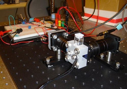
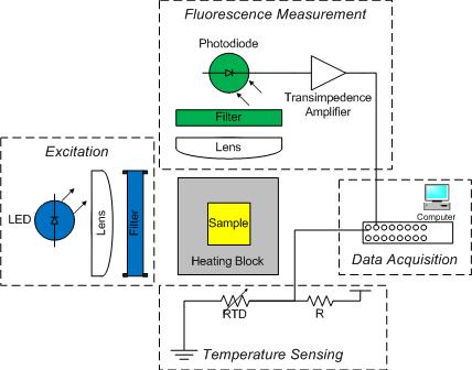
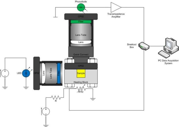
The DNA melting apparatus you will construct consists of four major subsystems: excitation, fluorescence measurement, temperature sensing, and data acquisition. You will build these subsystems out of an LED, a photodiode, a resistance temperature detector (RTD), and a PC data acquisition system.
The goal of your time in the lab will be to measure fluorescence intensity versus temperature for each of the samples over a range of about 90°C to room temperature. This will provide a basis for estimating the melting temperature, Tm of each sample. (Tm is defined as the temperature where half of the DNA in the sample remains hybridized.)
Three of the samples will be unknown. All the unknowns will have the same length, but different degrees of complementarity: complete match, single mismatch, and complete mismatch. Using the data you gather, you will attempt to identify these three samples.
Overview of the apparatus
SYBR Green I is a fluorescent dye with peak sensitivity to 498 nm blue light. The dye emits green light with a wavelength of 522 nm.[1] You can easily observe this – a room-temperature sample of dsDNA and SYBR green looks yellow from the combination of blue excitation and green fluorescence. At higher temperatures, when there is no dsDNA for the dye to bind to, the sample will appear blue or clear. In order to produce a melting curve, your apparatus will measure the amount of fluorescent emission from the SYBR Green dye over a range of temperatures.
Temperature will be measured by an RTD, which is a kind of resistor that predictable varies in value with temperature. Fluorescence intensity will be measured by a photodiode (and associated optical system). The sample will be heated by a thermoelectric device. A computer data acquisition system will record the signals from the photodiode and RTD. These signals must be processed to convert them from raw quantities to temperature and relative dsDNA concentration. The melting temperature, Tm can be estimated from a graph of this data or its derivative.
As shown in the diagram, an aluminum heating block holds a cuvette containing the sample under test. The sample is a combination of DNA and a fluorescent dye called SYBR Green. In addition to being a convenient holder, the block gives the setup enough thermal inertia to facilitate a measurement from natural cooling. (Without the block, the sample would cool too quickly.)
Blue light from an LED illuminates one side of the cuvette. An optical filter shapes the output spectrum of the LED so that only the desired wavelengths of light fall on the sample.
A photodiode placed at 90 degrees to the LED source detects the green light emitted by bound SYBR Green. The photodiode is placed behind an optical filter to ensure that only the fluorescent light given off by the sample is detected.
Since photodiodes produce only a very small amount of current, it will be necessary to build a very high gain transimpedence amplifier to produce a signal that is measurable by the PC data acquisition cards. Photodiode amplifiers are particularly challenging because many of the non-ideal characteristics of op amps become apparent at high gain.
An RTD attached to the heating block and wired to a voltage divider provides an indication of temperature. The temperature of the heating block will be a proxy for the sample temperature. Unfortunately, the block cools faster when it is hot than when it is near room temperature. You will have to get the heating block set up in your apparatus quickly after you remove it from the heating block.
A PC data acquisition card digitizes the amplified photodiode and RTD signals. A LabVIEW virtual instrument (VI) records the signals over time. Data from the DNA melting VI can be saved to a file. The file can be loaded into Matlab for analysis.
Objectives and learning goals
- Measure temperature with an RTD.
- Implement a high gain transimpedence amplifier for photodiode current multiplication.
- Measure light intensity with a photodiode.
- Build an optical system for exciting the sample with blue light and gathering the fluorescence output on the photodiode.
- Record dsDNA concentration versus temperature curves for several samples.
- Estimate Tm from your data.
- Compare the measured curves with theoretical models.
- Identify unknown DNA samples.
Lab procedure
Roadmap
- Build an optical system containing the LED, heating block, sample, photodiode, filters, and lenses.
- Hook up a three terminal voltage regulator to create an electrical power supply for the LED.
- Build, test, and calibrate the temperature-sensing circuit.
- Build an amplification/offset circuit for the DNA fluorescence signal.
- Troubleshoot and optimize your system.
- Heat a samples of DNA with SYBR Green dye and record DNA melting curves as the samples cool.
- Analyze the data. Identify the three unknown samples. Compare your observations to theoretical models.
Optical system
The optical system consists of an LED, excitation filter, sample cuvette, heating block, emission filter, photodiode, optional lenses, and associated mounting hardware. Construct your system on an optical breadboard. The breadboard has a grid of tapped holes for mounting all kinds of optical and mechanical hardware. ThorLabs manufactures most of the hardware stocked in the lab. A few of the components you will certainly use include: 1/2" diameter posts, CP02 cage plates, and 1” diameter lens tubes.
Use optical rails and rail carriers or optical bases to mount 1/2” posts on the breadboard. RA90 right angle post clamps and post holderscan also be useful.
There are a variety of ways to construct the apparatus. A good design will be compact, stable, and simple. It will be necessary to shield the optical system from ambient light, so a small footprint will be advantageous.
Illumination
Begin by mounting the LED on your breadboard. Note that there are two styles of LEDs. The Lamina LED Array is mounted on an aluminum heat sink and bolted to a CP02 cage plate. The CP02 attaches to the top of a post. It has an SM1 threaded hole through the middle that connects to 1” diameter lens tubes. The Cree LEDs are already mounted in a 1” lens tube.
Both styles of LED emit a range of wavelengths with a peak at 475 nm. A Chroma Technology D470 filter eliminates unwanted parts of the spectrum that might interfere with detection of the fluorescence signal. The filters have exposed, delicate coatings and must be handled carefully. In addition, the filter works better in one direction than the other.
Light from both kinds of LEDs diverges in a cone with an angle of about 100 degrees, so place the device close to the sample. You can also use a lens to concentrate the LED's output. Several lenses are available in the lab:
Fluorescence detection
The SM05PD1A photodiode is mounted in a short tube with SM05 threads. Use a SM1A6 adapter to mount the photodiode in a CP02 cage plate. Mount the photodiode assembly to the breadboard at 90 degrees to the LED. Build a system to hold the Chroma E515LPV2 emission filter in front of the photodiode. You can use a lens to focus light from the sample on to the detector to improve performance, if you like.
Put an optical quick connect at the end of the photodiode assembly to facilitate easy attachment of the heating block during experimental runs. The other half of the quick connect goes into the CP02 cage plate mounted on the heating block.
Electrical System
Temperature
The electrical resistance of most materials varies with temperature. RTDs are a special resistors (usually made out of platinum) that exhibit a nearly linear change in its value with temperature. An RTD may be used to accurately measure temperature by including it as an element in a voltage divider. As the resistance of the RTD changes, so will the voltage across it.
A PPG102A1 RTD has been pre-mounted to the DNA heating block. This RTD has a nominal resistance of 1 KΩ and its value increses with temperature. Note that the maximum current carrying capacity of this device is 1 ma. Hook up the RTD in a voltage divider. Make sure the divider has no more than 1 mA flowing through it. Use freeze spray or heat the block on the warmer to test the circuit.
LED driver
Or: how to make a current source
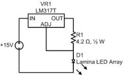
Drive the LED array with an LM317T variable voltage regulator as shown. The LM317T has a feedback circuit that strives to maintain 1.25 volts between its output and adjustment pins. Thus, in the circuit shown, the LM317T sources a constant current of approximately .29A through the load (and the feedback resistor).
It is possible to drive an LED with a voltage source; however, the steepness of a diode's I-V curve results in large current swings in current for small changes in supply voltage. LED brightness is proportional to current, so a current source tends to provide a more stable light output.
The LM317T and 4.3Ω resistor both dissipate quite a bit of power in this connection. They will become toasty. Use a heat sink on the LM317T. Double check your wiring before connecting the LED array. The array can be damaged by excessive current. Remember the rule of finger: if you can't keep your finger on a component indefinitely, it is too hot. Use a larger feedback resistor to keep the electronics cooler (at the expense of light output), but never a smaller one.
Photodiode amplifier
Excited SYBR Green molecules emit photons in all directions, some of which pass through the emission filter and strike the photodiode. This generates a tiny current, which must be converted to a voltage and amplified to a level that can be conveniently measured. In order to determine the requirements for the amplifier, it is helpful to estimate the amount of current that will be produced by the photodiode.
Estimating photodiode current
The current output of the photodiode depends on several factors: illumination intensity, illumination system efficiency, fluorophore absorption and quantum yield, optical system collection efficiency, and photodiode quantum efficiency. Many of these quantities are difficult to know precisely, so a back-of-the-envelope calculation will have to suffice. You will probably need to fine tune your amplifier gain after the system is assembled.
- $ I_{PD} \approx P_{LED} \; A_{LED} \; \alpha_{fluor} \; \phi_{fluor} \; A_{diode} \; \phi_{diode} $
- where,
- PLED is the LED power, about 0.5 W = 2.5 * 1019 photons/sec,
- ALED is the efficiency of Illumination system, about 0.1, considering the spectral output of the LED, filter, lens, etc...,
- αfluor is the SYBR Green absorption coefficient (approximately 0.85, estimated using Beer's law for a system with path length = 1cm, dsDNA concentration = 1μM, and a molar absorption coefficient for SYBR Green I of 73x103)[2]
- φfluor is the quantum yield of SYBR Green, about 0.8 [3]
- Adiode is the optical system collection efficiency, about 0.1
- φdiode is the photodiode quantum efficiency, typically around 0.8 electrons per photon
Substituting the guesses gives an estimate of about 16 nanoamps full scale current.
Amplification circuit
The DAQ system can digitize a voltage between positive and negative 10 Volts. A transimpedance amplifier (sometimes called a current-to-voltage converter) with a gain of approximately 6x10⁸ V/A will produce an output that approximately matches this range, given a 16 nanoamp input. The circuit considered in Homework 1 is capable of providing this gain. (Why not simply use a resistor, and omit the op-amp?)
Photodiode amplifiers can be fiddly under the best of circumstances. At such high gain, many of the non-ideal behaviors of op amps become apparent. It will be important to keep your wiring short and neat. The amplifier and witing will also be susceptible to physical movement, so prevent things from getting bumped during experimental runs. In addition select an op amp that has a very low input bias current as possible. (Why?) Op amps with JFET inputs like the LF411 and LF351 generally have the lowest input current.
Offset circuit
The positive and negative input channels of an op amp cannot be perfectly matched during manufacturing. Because the open loop gain of an op amp is huge — usually 105 or more — even a slight mismatch will cause a non-ieal behavior called input offset voltage. (In other words, if you apply a zero voltage to the across the plus and minus pins by shorting them together, the output will probably saturate at the full positive or negative output limit.) Vos is the voltage that must be applied across the inputs to achieve a zero output. Most op amp datasheets specify a maximum value for Vos. In terms of the ideal circuit elements, input offset acts like a small voltage source connected in series with one of the input pins. As a real world example, the maximum specified offset voltage of the LF411 is 2.0 mV.
In the lab, you will find it useful to be able to adjust the quiescent output level of the photodiode amplifier. Many op amps provide a means for externally balancing the mismatch between plus and minus inputs. Pins 1 and 5 of both the LF351 and the LF411 are connected to the current sources that drive the differential input stage. As suggested by the name, these balance pins allow slight changes in the balance of current flowing through each side of the input stage. A potentiometer with both ends hooked across these pins and the wiper hooked to the negative supply voltage allows Vos to be virtually eliminated with a single adjustment. See the Typical Connection schematic diagram on page 1 of the LF411 datasheet.
Although the primary intent of the balance pins is to null out Vos, they will also work quite nicely as an output level adjustment. Use a 10 turn pot so that you can get the output to settle where you want it. Adjust the dark output of the amplifier to be approximately zero.
Unfortunately, input offset voltage varies with temperature. (The LF411, for example, specifies a maximum temperature coefficient of 20μV/°C.) This sensitivity is one of the chief causes of output drift in the high gain amplifier, which you will undoubtedly notice in the lab. Try spraying a little freeze spray on the op amp to observe the effect. (Don’t freeze your op amp right before you do an experimental run — it takes quite a while to stabilize.)
Practical matters
As with most amplifiers, care should be taken with lead dress, component placement and supply decoupling in order to ensure stability.
In theory, there is no difference between theory and practice. But, in practice, there is.
The universe is rife with electrical noise. Keeping the noise out of sensitive electronic instruments requires a great deal of care. Unfortunately, electronic breadboards are a poor environment in which to construct high gain amplifiers. A few simple tricks can improve things.
- Strap the ground of your breadboard to the optical table by connecting it with a short wire to a screw in the table.
- Use power supply bypass capacitors. Connect a large capacitor between all supply voltges and ground. Large, electrolytic capacitors of at least 0.1 μFd work well for this purpose. Electrolytic capacitors are polarized. Make sure to put them in the right direction.
- What happens when the shield of a BNC cable touches the optical table? If you notice an effect, take precautions to prevent this from happening during an experimental run.
- Move your hands around dfferent parts of the circuit. What effects do you see?
PC Data Acquisition System
Each lab PC is equipped with a National Instruments USB-6212 or USB-6341 data acquisition (DAQ) card.
The USB-6212[4] has 16, 16-bit analog input channels which can, in sum total, accomplish 400 thousand samples per second (400kS/s). That is, if there are two channels, each one will be alternately sampled, and EACH sampled at 200kS/s. A multiplexer sequentially selects from among the 16 single-ended and 8 differential input signals. The card also supports two 16 bit analog output channels with an update rate of 250 kS/s and an output range of +/-10 V and up to +/-2 mA.
The USB-6212 also has 32 digital input/output channels and a digital ground. A 50 kΩ pull-down resistor is typically used in series with connections to these channels.
The USB-6341[5] is s little more powerful. It has 16, 16-bit analog input channels which can, in sum total, accomplish 500 thousand samples per second (500kS/s). Again, a multiplexer sequentially selects from among the 16 single-ended and 8 differential input signals. The card also supports two 16 bit analog output channels but they have an update rate of 900 kS/s and an output range of +/-10 V and up to +/-2 mA.
Finally, the USB-6341 has 24 digital input/output channels and a digital ground, as well as 4, 100 MHz counter/timers.
LabVIEW VI
The DNA Melting LabVIEW VI is located in the Students/Labs/DNA Melting folder of the course locker. Double click to launch the VI. (The current version is R1.0)
Click the run arrow or select Operate->Run from the menu to start the VI. The top two charts show the digitized voltage at the RTD and diode inputs over time. Use the range settings to get a good view of the signal.
Press Start Recording to begin taking data. The sample rate for recorded data can be set in increments of 0.1 seconds. Press Stop Recording at the end of an experimental run and use the Write Data button to save the most recent result in a comma delimited file that can be read into Matlab or Excel.
Debugging the apparatus
- Use freeze spray and the heat gun to make sure the temperature circuit is working properly.
- Cover and uncover the photodiode to verify operation of the fluorescence measurement system.
- Use a box and a piece of black cloth to shield your apparatus from ambient light. Can you measure the difference between a cuvette filed with water and one with DNA and SYBR Green?
- Observe every electrical signal node with the oscilloscope. Are any signals noisy? Is there a way to improve the quality of poor signals?
- Watch the fluorescence readout over time. Is it stable or does it drift?
Experimental procedure
Once your instrument is running to your satisfaction, measure melting curves each of the 5 conditions:
- 40bp perfect match
- 3 unknown 20 bp sequences (perfect match, single mismatch, and complete mismatch)
- 20 bp perfect match at different ionic strength
If you have time, you can run additional experiments. For example, you could gather additional ionic strength data points.
The DNA melting apparatus will generate the best data when both the amplifier circuit and LED have been on for a while and all the components have reached their steady state temperature. Make sure the outupts of the system are stable before you begin taking data. Turn your apparatus on and measure the difference between a cool DNA sample and water. Run the DNA melting LabVIEW VI in the DNAMelting directory of the course locker. Adjust the range controls for each channel to provide the greatest measurement resolution.
The steps for each experimental run are:
- Heat up the sample on the hot plate
- Quickly transfer the sample to your setup
- Cover the apparatus to block out ambient light
- Start recording RTD and photodiode output with the LabVIEW VI.
- Wait for the block to cool to below 40°C
Prepare your apparatus
Use the potentiometer to adjust the amplifier voltage offset until it reads close to 0 Volts in the dark. Make sure your apparatus has reached the steady state and the fluorescence readout is stable.
Make a sample
Pipet 500μl of DNA plus dye solution into a disposable plastic cuvette. Pipet 20μl of mineral oil on top of the sample to help prevent evaporation. Put a top on the cuvette and mark it with a permanent marker. Keep the sample vertical to make sure the oil stays on top. You should be able to use the same sample for many heating/cooling cycles. Only discard it if you lose significant volume due to evaporation. If you need to leave the sample overnight, store it in the lab refrigerator. If you finish with a sample and it is still in good shape, pass it on to another group.
Heat up the sample
Place your heating block and sample in the hot water bath. You can use a DVM to monitor the temperature of the holder. It takes longer than you think to reach equilibrium. The block will cool down a bit while you transfer it to your setup, so heat it to a temperature well above where the DNA melts (at least 85°C, preferably 90°C). The double boiler arrangement will not allow the sample to boil.
Transfer the sample to your apparatus and take data
Use tongs to remove the heating block from the bath. Remember to keep everything upright. Set the block down on a paper towel. Use leather gloves to pick up the sample and connect it optically and electrically to your apparatus. Once everything is hooked up, press the Start Recording button on the LabView DNA Melting VI.
Data Analysis
Use Matlab or another environment of your choosing to analyze the raw data. In outline, the steps are:
- Load data file produced by LabVIEW VI into Matlab
- Apply median filter to reduce impulse noise
- Apply FIR filter to reduce technical noise
- Convert RTD voltage to temperature
- Normalize fluorescence signal
- Sort or bin the data to ensure that fluorescence versus temperature is a function
- Compute the finite difference Δfluorescence/Δtemperature
- Estimate the melting temperature
- Create plots
Organization of the data analysis script
Since you will be analyzing several experimental runs in a similar way, it makes sense to save the particulars of each sample in an array of data structures. Matlab implements a data type called a cellular array. Cellular arrays use pointy braces {} instead of parenthesis (). If foo is a cellular array, foo{1} is the first element.
Each data structure contains information about the experimental such as the file name and the DNA concentration. The script is surrounded by a for loop that runs the analysis on each dataset, something like this:
% Function to process DNA melting data from LabVIEW VI
% sampleInfo is a cellular array of data structures
% output is a cellular array containing original data and computed values
function out = DnaMelt(sampleInfo)

% initialize variables
out = {};

for ii=1:length(sampleInfo)
<br />
:''... process the data
<br />
end
The following code demonstrates how to make the cellular array of data structures. The code fills in the first element of the cellular array DnaMatchSampleInfo:
DnaMatchSampleInfo = {}  % null cellular array

DnaMatchSampleInfo{1}.filename = 'DNA Melting Data\20bp 100mM.txt';
DnaMatchSampleInfo{1}.SampleName = '20 bp 100mM';
DnaMatchSampleInfo{1}.KclConcentration = 100;
DnaMatchSampleInfo{1}.DnaConcentration = 30;
DnaMatchSampleInfo{1}.FilterNormalizedCutoffFrequency = 0.1;
DnaMatchSampleInfo{1}.FilterOrder = 25;
DnaMatchSampleInfo{1}.NormalizationMin = 0.01;
DnaMatchSampleInfo{1}.NormalizationMax = 0.99;
DnaMatchSampleInfo{1}.TrimStart = 0;
DnaMatchSampleInfo{1}.TrimEnd = 0;
Loading a data file
Use the load command to read in a data file.
rawData = load(sampleInfo{ii}.filename);
The first column contains RTD voltage samples and the second contains the corresponding fluorescence voltages.
Converting voltages to temperature and relative fluorescence
These are straightforward mathematical manipluations on the dataset.
Designing an FIR low pass filter
The matlab commands fir1 and freqz are useful for designing a low pass filter. Use fir1 to generate the filter kernel and freqz to plot its frequency response. Increasing the order of the filter will make the transition between pass and stop bands more abrupt.
Try plotting a few different filter designs:
freqz(fir1(30, 0.15))
freqz(fir1(300, 0.15))
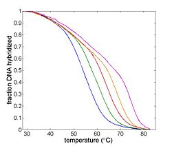
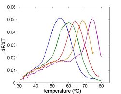
Use Matlab to convert your raw data to fraction hybridized and temperature. (Can you learn anything from the absolute value of the photodiode output?) Filter the data to remove noise. This can involve smoothing the data from individual experimental runs as well as combining data from multiple runs. Plot relative fluorescence versus temperature comparing:
- 20 bp oligos in solutions of varying ionic strength
- Perfect match, single mismatch, and complete mismatch (unknown) 20 bp oligos
- 40 bp versus 20 bp perfect match oligos
In addition, plot the derivative of each curve. Note that the differentiation operation is particularly sensitive to noise. If your derivative plots look noisy, apply better filtering to the raw data. It will be helpful to create a matlab script to process the data. Tm is taken to be the peak value of the derivative.
You may process the data how you wish, however a useful command in Matlab is resample . This function can not only resample data, as the name implies, but will also apply a low-pass filter (decreasing the high-frequency noise). A larger vector of filter coefficients or number of samples on each side of the current sample will smooth the data more. Using this command, pay attention to the resulting length of your new data, as well as any inaccuracies at the ends (what does resample assume for the data points before and after your data?). Derivatives may require filtering as well.
Model vs. reality
In class, we derived an expression that relates the melting temperature to the enthalpy change ΔH° and entropy change ΔS° of the hybridization reaction:
$ T(f) = \frac{\Delta H^{\circ}}{\Delta S^{\circ}-R \ln (2f/C_T(1-f)^2)} $.
Here, $ f $ is the fraction of DNA strands hybridized (dimerized) at a particular temperature (at $ T_m $, this is 1/2), and $ C_T $ is the total concentration of single-strand oligonucleotides (or 2X the dsDNA concentration when all strands are hybridized). Choose one of the perfect-match sequences that you measured, and use matlab to fit the model to your measured data, which will allow you to extract the ΔH° and ΔS° parameters. To perform the fit, you will need a matlab function that will evaluate $ T(f) $ given an input const for the ΔH° and ΔS° parameters. The function will be something like this:
function Tf = melt(const, f)
R=8.3;
C_T=33e-6;
dH = const(1);
dS = const(2);
Tf = dH./(dS - R*log(2*f./(C_T*(1-f).^2)));
You can then invoke matlab's lsqcurvefit routine to do the fit, which will return the best values for ΔH° and ΔS°.
FitVals = lsqcurvefit(@melt, [dH_guess, dS_guess], frac_vector, temp_vector)
Report Requirements
Report outline
Use the following format for your report:
- Results
- Samples run
- List all of the samples you characterized (length/ionic strength)
- Data plots
- All plots should be complete with title, axis labels, and legend. Plot both your experimental data and the best fit curves from the DNA melting mode. Plots in this section should include only data that was created by your group's own hands in the lab. Analysis of other people's datasets belongs in a different section (see below).
- Single set of axes with plots of dsDNA concentration versus temperature for the 20 base pair complementary, single mismatch, and complete masmatch samples.
- Single set of axes with plots of ΔdsDNA concentration/Δtemperature for the 20 base pair complementary, single mismatch, and complete masmatch samples.
- Single set of axes with plots of dsDNA concentration versus temperature for the ionic strength or oligo length samples you measured.
- Single set of axes with plots of ΔdsDNA concentration/Δtemperature for the ionic strength or oligo length samples you measured.
- Table of estimated thermodynamic parameters
- Include estimated ΔH, ΔS, and Tm values (by multiple methods)
- Comparative data analysis and plots
- Plots of any data you analyzed that came from other groups
- Data analysis overview
- Bullet point summary of your data analysis methodology.
- Discussion of results
- Bullet point discussion of results. Compare your results to theoretical models and/or other group's datasets. Be concise, but express yourself clearly.
- Sources of error
- List sources of error. Indicate whether each source causes a systematic or random distortion in the data. (The uncertainty from a random error decreases with additional experimental runs; systematic error does not.)
- Instrument documentation
- Block diagram
- Include component values, relevant distances, and possibly a photographs or two. It is not necessary to document construction details.
- Signal to noise measurement
- Divide the signal magnitude (size of the signal with a reference sample minus the size with a null sample such as water) by the average
- Design evolution
- Bullet point summary of changes you made to your instrument design to address problems in the lab.
References
- ↑ SYBR Green I online datasheet
- ↑ <a href=" http://www.pubmedcentral.nih.gov/articlerender.fcgi?artid=484200">Zipper H, Brunner H, Bernhagen J, Vitzthum F. Investigations on DNA intercalation and surface binding by SYBR Green I, its structure determination and methodological implications. Nucleic Acids Res. 2004;32:e103–10.</a>
- ↑ From SYBR Green online datasheet SYBR Green Datasheet
- ↑ Datasheet for the USB-6212
- ↑ Datasheet for the USB-6341
