Assignment 7, Part 1: op amp golden rules questions

This is Part 1 of Assignment 7.
| |
Turn in your answers to the following questions |
- Op amp circuits:
-
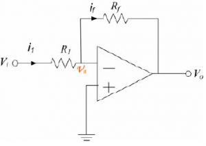

(a) Inverting voltage amplifier Calculate the gain of circuit (a), Vo / Vi, in terms of the input voltage and the two resistor values.
-
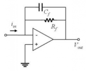
(b) Transimpedance amplifier at DC (C = 0) In the DNA melting lab, fluorescence intensity will be determined by measuring the output current of a photodiode. Schematic (b) shows a circuit called a transimpedance amplifier that converts a current to a voltage.
Derive an expression for the output voltage of the circuit produced by a DC current input at iin (b). (At DC, you can ignore the effect of the capacitor.) Express your answer in the form of a transfer function, Vout / iin. - What is the high frequency gain of the transimpedance amplifier shown in Schematic (b)? Remember that a capacitor acts like an open circuit at low frequencies and a short circuit at high frequencies.
- A transimpedance amplifier with a gain of approximately -106 V/A will be required for the DNA melting lab. What value of resistor in the circuit (b) would achieve this gain?
-
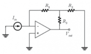
(c) High gain transimpedance amplifier It is undesirable to use the large value of resistor you computed in part A.4. Shown in (c) is another possible implementation of the transimpedance amplifier. Derive an expression for the output voltage of this circuit in terms of the input current and the three resistor values.
- In part A.3., you determined the effect of putting a capacitor across the feedback resistor in a transimpedance amplifier. High gain amplifiers are susceptible to noise coupling from a variety of sources. Since high frequencies are not of interest in the DNA melting lab, it is beneficial to insert a capacitor to reduce the noise. In circuit (c), where would you connect the capacitor and how would you choose its size?
- Now work out the expression for this new circuit's output with respect to the current input for AC signals.
-
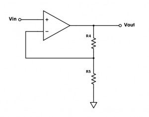
(d) Voltage amplifier op amp circuit Unfortunately, when the gain of an op amp circuit is very high (i.e. higher than ~106 V/A), we can no longer ignore the non-idealities of the op amp, and the circuit starts to misbehave. If we want to increase the gain beyond this limit, we can add an additional amplification stage to our circuit (Schematic (d)). Solve for the gain, Vout / Vin, of the circuit in Schematic (d) in terms of the input voltage and the two resistor values, R4 and R5.
-
- Simulating DNA melting lab:
- Using DINAmelt or your favorite DNA melting calculator, find an estimate for ΔH0 and ΔS0 for the following oligonucleotide sequence: ATC AAG CAG CCA TCG AAA AAA CT. Assume the complementary strand has no mismatches, the sodium concentration is 100 mM, and the total concentration of oligonucleotide strands is 60 μM.
-
In class, we derived an equation to describe the fraction (f) of double-stranded DNA in solution as a function of temperature (T) in Kelvin as shown below:
$ f = {1 + C_T K_{eq} - \sqrt{(1 + 2C_T K_{eq})} \over C_T K_{eq}} $
CT is the total concentration of oligonucleotide strands (60 μM), and Keq is the equilibrium constant as described by the following equation:
$ K_{eq} = e^{ [{\Delta S^0 \over R} - { \Delta H^0 \over RT }]} $
Using these equations and the values you found in part 1, simulate a DNA melting curve, plotting f vs. T. Feel free to use the MATLAB functions given on the wiki page:
http://measurebiology.org/wiki/DNA_Melting:_Simulating_DNA_Melting_-_Basics
- Measuring temperature with an RTD
- In Part 2 of this assignment, you will measure temperature using an RTD - a temperature dependent resistor. The resistance of the RTD varies with temperature according to the equation RRTD = 1000 Ω + 3.85 θ, where θ is the temperature of the RTD in degrees Celsius. If your RTD is set up in series with a 15 kΩ resistor and a 15 V power supply (as shown in the figure to the right), what voltage would you expect to measure across the RTD (VRTD) at room temperature (21 C)?
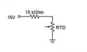 RTD circuit
 - Find an equation for the block temperature, θ, as a function of the voltage across the RTD, VRTD.
- Above we assumed the source voltage was 15V exactly. How is the temperature calculation affected by a 1% change in the 15 V input voltage? In other words, if you assume the same measured voltage across the RTD as in Question C.1, but have a 1% change in the input voltage, how much does your calculated temperature change? Note the importance of keeping track of your input voltage.
-


- Overview
- Part 1: Pre-lab problems
- Part 2: Build an instrument to measure temperature and fluorescence
- Part 3: Testing and measuring stuff
Back to 20.309 Main Page